Cyrix 6x86
This article includes a list of general references, but it remains largely unverified because it lacks sufficient corresponding inline citations. (September 2011) |
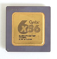 A Cyrix 6x86-P166 processor | |
| Cache | |
|---|---|
| L1 cache | 16 KB (6x86/L) or 64 KB (6x86MX / MII) |
| Architecture and classification | |
| Microarchitecture | 6x86 |
| Instruction set | IA-32/x86 |
| Physical specifications | |
| Transistors |
|
| Cores |
|
| Socket(s) | |
| Products, models, variants | |
| Model(s) |
|
| History | |
| Predecessor | Cyrix Cx486 |
The Cyrix 6x86 (codename M1) is a sixth-generation, 32-bit x86 microprocessor designed by Cyrix and manufactured by IBM and SGS-Thomson. It was originally released in 1996.
Architecture[]

The 6x86 is superscalar and superpipelined and performs register renaming, speculative execution, out-of-order execution, and data dependency removal.[1] However, it continued to use native x86 execution and ordinary microcode only, like Centaur's Winchip, unlike competitors Intel and AMD which introduced the method of dynamic translation to micro-operations with Pentium Pro and K5. The 6x86 is socket-compatible with the Intel P54C Pentium, and was offered in six performance levels: PR 90+, PR 120+, PR 133+, PR 150+, PR 166+ and PR 200+. These performance levels do not map to the clock speed of the chip itself (for example, a PR 133+ ran at 110 MHz, a PR 166+ ran at 133 MHz, etc.).
With regard to internal caches, it has a 16-KB primary cache and a fully associative 256-byte instruction line cache is included alongside the primary cache, which functions as the primary instruction cache.[1]
The 6x86 and 6x86L weren't completely compatible with the Intel P5 Pentium instruction set and is not multi-processor capable. For this reason, the chip identified itself as a 80486 and disabled the CPUID instruction by default. CPUID support could be enabled by first enabling extended CCR registers then setting bit 7 in CCR4. The lack of full P5 Pentium compatibility caused problems with some applications because programmers had begun to use P5 Pentium-specific instructions. Some companies released patches for their products to make them function on the 6x86.
Compatibility with the Pentium was improved in the 6x86MX, by adding a Time Stamp Counter to support the P5 Pentium's RDTSC instruction.[2] Support for the Pentium Pro's CMOVcc instructions were also added.[2]
Performance[]
Similarly to AMD with their K5 and early K6 processors, Cyrix used a PR rating (Performance Rating) to relate their performance to the Intel P5 Pentium (pre-P55C), as the 6x86's higher per-clock performance relative to a P5 Pentium could be quantified against a higher-clocked Pentium part. For example, a 133 MHz 6x86 will match or outperform a P5 Pentium at 166 MHz, and as a result Cyrix could market the 133 MHz chip as being a P5 Pentium 166's equal. However, the PR rating was not an entirely truthful representation of the 6x86's performance.
While the 6x86's integer performance was significantly higher than P5 Pentium's, its floating point performance was more mediocre—between 2 and 4 times the performance of the 486 FPU per clock cycle (depending on the operation and precision). The FPU in the 6x86 was largely the same circuitry that was developed for Cyrix's earlier high performance 8087/80287/80387-compatible coprocessors, which was very fast for its time—the Cyrix FPU was much faster than the 80387, and even the 80486 FPU. However, it was still considerably slower than the new and completely redesigned P5 Pentium and P6 Pentium Pro-Pentium III FPUs.
During the 6x86's development, the majority of applications (office software as well as games) performed almost entirely integer operations. The designers foresaw that future applications would most likely maintain this instruction focus. So, to optimize the chip's performance for what they believed to be the most likely application of the CPU, the integer execution resources received most of the transistor budget. This would later prove to be a strategic mistake, as the popularity of the P5 Pentium caused many software developers to hand-optimize code in assembly language, to take advantage of the P5 Pentium's tightly pipelined and lower latency FPU. For example, the highly anticipated first person shooter Quake used highly optimized assembly code designed almost entirely around the P5 Pentium's FPU. As a result, the P5 Pentium significantly outperformed other CPUs in the game.
Therefore, despite being very fast clock by clock, the 6x86 and MII were forced to compete at the low-end of the market as AMD K6 and Intel P6 Pentium II were always ahead on clock speed. The 6x86's and MII's old generation "486 class" floating point unit combined with an integer section that was at best on-par with the newer P6 and K6 chips meant that Cyrix could no longer compete in performance.
Models[]
6x86[]

The 6x86 (codename M1) was released by Cyrix in 1996. The first generation of 6x86 had heat problems. This was primarily caused by their higher heat output than other x86 CPUs of the day and, as such, computer builders sometimes did not equip them with adequate cooling. The CPUs topped out at around 25 W heat output (like the AMD K6), whereas the P5 Pentium produced around 15 W of waste heat at its peak. However, both numbers would be a fraction of the heat generated by many high performance processors, some years later.


Early Cyrix 6x86 (M1) die shot

6x86L[]

The 6x86L (codename M1L) was later released by Cyrix to address heat issues; the L standing for low-power. Improved manufacturing technologies permitted usage of a lower Vcore. Just like the Pentium MMX, the 6x86L required a split powerplane voltage regulator with separate voltages for I/O and CPU core.

Cyrix 6x86L (M1L) die shot

6x86MX / MII[]


Another release of the 6x86, the 6x86MX, added MMX compatibility along with the EMMI instruction set, improved compatibility with the Pentium and Pentium Pro by adding a Time Stamp Counter and CMOVcc instructions respectively, and quadrupled the primary cache size to 64 KB. The 256-byte instruction line cache can be turned into a scratchpad cache to provide support for multimedia operations.[2] Later revisions of this chip were renamed MII, to better compete with the Pentium II processor. Unfortunately, 6x86MX / MII was late to market, and couldn't scale well in clock speed with the manufacturing processes used at the time.
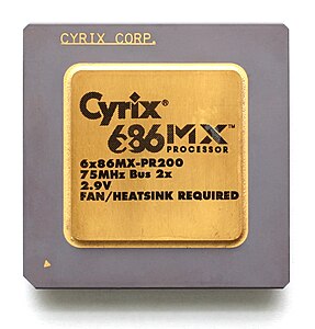
Cyrix 6x86MX 150 MHz

IBM 6x86MX 133MHz
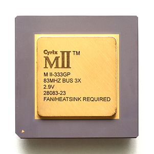
Cyrix MII 250MHz

Cyrix 6x86MX (M2) die shot


References[]
- ^ Jump up to: a b "Cyrix M1 datasheet" (PDF).
- ^ Jump up to: a b c "IBM 6x86MX datasheet" (PDF).
Further reading[]
- Gwennap, Linley (October 25, 1993). "Cyrix Describes Pentium Competitor" Microprocessor Report.
- Gwennap, Linley (December 5, 1994). "Cyrix M1 Design Tapes Out". Microprocessor Report.
- Gwennap, Linley (June 2, 1997). "Cyrix 6x68MX Outperforms AMD K6". Microprocessor Report.
- Slater, Michael (February 12, 1996). "Cyrix, IBM Push 6x86 to 133 MHz". Microprocessor Report.
- Slater, Michael (October 28, 1996). "Cyrix Doubles x86 Performance with M2". Microprocessor Report.
External links[]
- Cyrix 6x86 ("M1") at PCGuide at the Wayback Machine (archived June 22, 2017)
- Cyrix 6x86 ("M1") at PCGuide
- cpu-collection.de Cyrix 6x86 processor images and descriptions
- Paul Hsieh's 6th Generation x86 CPU Comparison in-depth analysis of 6th generation x86 CPUs, including the 6x86MX.
- Cyrix M1 stats at Sandpile.org
- Cyrix x86 microprocessors
- Superscalar microprocessors