Integrated circuits are put into protective packages to allow easy handling and assembly onto printed circuit boards and to protect the devices from damage. A very large number of different types of package exist. Some package types have standardized dimensions and tolerances, and are registered with trade industry associations such as JEDEC and Pro Electron. Other types are proprietary designations that may be made by only one or two manufacturers. Integrated circuit packaging is the last assembly process before testing and shipping devices to customers.
Occasionally specially-processed integrated circuit dies are prepared for direct connections to a substrate without an intermediate header or carrier. In flip chip systems the IC is connected by solder bumps to a substrate. In beam-lead technology, the metallized pads that would be used for wire bonding connections in a conventional chip are thickened and extended to allow external connections to the circuit. Assemblies using "bare" chips have additional packaging or filling with epoxy to protect the devices from moisture.
Through-hole technology uses holes drilled through the PCB for mounting the components. The component has leads that are soldered to pads on the PCB to electrically and mechanically connect them to the PCB.
Three 14-pin (DIP14) plastic dual in-line packages containing IC chips.
A chip carrier is a rectangular package with contacts on all four edges. Leaded chip carriers have metal leads wrapped around the edge of the package, in the shape of a letter J. Leadless chip carriers have metal pads on the edges. Chip carrier packages may be made of ceramic or plastic and are usually secured to a printed circuit board by soldering, though sockets can be used for testing.
A WL-CSP or WLCSP package is just a bare die with a redistribution layer (or I/O pitch) to rearrange the pins or contacts on the die so that they can be big enough and have sufficient spacing so that they can be handled just like a BGA package.[20]
PMCP
Power mount CSP (chip-scale package)
Variation of WLCSP, for power devices like MOSFETs. Made by Panasonic. [21]
Bare die supplied without a package. It is mounted directly to the PCB using bonding wires and covered with a blob of black Epoxy.[23] Also used for LEDs. In LEDs, transparent epoxy or a silicon caulk-like material that may contain a phosphor is poured into a mold containing the LED(s) and cured. The mold forms part of the package.
COF
Chip-on-flex
Variation of COB, where a chip is mounted directly to a flex circuit. Unlike COB, it may not use wires nor be covered with epoxy, using underfill instead.
Example of component sizes, metric and imperial codes and comparison included
Composite image of a 11×44 LED matrix lapel name tag display using 1608/0603-type SMD LEDs. Top: A little over half of the 21×86 mm display. Center: Close-up of LEDs in ambient light. Bottom: LEDs in their own red light.
SMD capacitors (on the left) with two through-hole capacitors (on the right)
Surface-mount components are usually smaller than their counterparts with leads, and are designed to be handled by machines rather than by humans. The electronics industry has standardized package shapes and sizes (the leading standardisation body is JEDEC).
The codes given in the chart below usually tell the length and width of the components in tenths of millimeters or hundredths of inches. For example, a metric 2520 component is 2.5 mm by 2.0 mm which corresponds roughly to 0.10 inches by 0.08 inches (hence, imperial size is 1008). Exceptions occur for imperial in the two smallest rectangular passive sizes. The metric codes still represent the dimensions in mm, even though the imperial size codes are no longer aligned. Problematically, some manufacturers are developing metric 0201 components with dimensions of 0.25 mm × 0.125 mm (0.0098 in × 0.0049 in),[32] but the imperial 01005 name is already being used for the 0.4 mm × 0.2 mm (0.0157 in × 0.0079 in) package. These increasingly small sizes, especially 0201 and 01005, can sometimes be a challenge from a manufacturability or reliability perspective.[33]
4.5 mm × 2.5 mm × 1.5 mm body: four terminals, center pin is connected to a large heat-transfer pad.[56]
SOT-143 (TO-253)
2.9 mm × 1.3 mm × 1.22 mm tapered body: four terminals: one larger pad denotes terminal 1.[57]
SOT-223 (TO-261)
6.5 mm × 3.5 mm × 1.8 mm body: four terminals, one of which is a large heat-transfer pad.[58]
SOT-323 (SC-70)
2 mm × 1.25 mm × 1.1 mm body: three terminals.[59]
SOT-416 (SC-75)
1.6 mm × 0.8 mm × 0.9 mm body: three terminals.[60]
SOT-663
1.6 mm × 1.2 mm × 0.6 mm body: three terminals.[61]
SOT-723
1.2 mm × 0.8 mm × 0.55 mm body: three terminals: flat lead.[62]
SOT-883 (SC-101)
1 mm × 0.6 mm × 0.5 mm body: three terminals: leadless.[63]
Other[]
DPAK (TO-252, SOT-428): Discrete Packaging. Developed by Motorola to house higher powered devices. Comes in three[64] or five-terminal[65] versions.
D2PAK (TO-263, SOT-404): Bigger than the DPAK; basically a surface mount equivalent of the TO220 through-hole package. Comes in 3, 5, 6, 7, 8 or 9-terminal versions.[66]
Quad flat package (QFP): various sizes, with pins on all four sides
Low-profile quad flat-package (LQFP): 1.4 mm high, varying sized and pins on all four sides
Plastic quad flat-pack (PQFP), a square with pins on all four sides, 44 or more pins
Ceramic quad flat-pack (CQFP): similar to PQFP
Metric quad flat-pack (): a QFP package with metric pin distribution
Thin quad flat-pack (TQFP), a thinner version of LQFP
Quad flat no-lead (QFN): smaller footprint than leaded equivalent
Leadless chip carrier (LCC): contacts are recessed vertically to "wick-in" solder. Common in aviation electronics because of robustness to mechanical vibration.
Micro leadframe package (MLP, MLF): with a 0.5 mm contact pitch, no leads (same as QFN)
Power quad flat no-lead (): with exposed die-pads for heatsinking
Grid arrays[]
Ball grid array (BGA): A square or rectangular array of solder balls on one surface, ball spacing typically 1.27 mm (0.050 in)
Fine-pitch ball grid array (FBGA): A square or rectangular array of solder balls on one surface
Low-profile fine-pitch ball grid array (LFBGA): A square or rectangular array of solder balls on one surface, ball spacing typically 0.8 mm
Micro ball grid array (): Ball spacing less than 1 mm
(TFBGA): A square or rectangular array of solder balls on one surface, ball spacing typically 0.5 mm
Land grid array (LGA): An array of bare lands only. Similar to in appearance to QFN, but mating is by spring pins within a socket rather than solder.
(CGA): A circuit package in which the input and output points are high-temperature solder cylinders or columns arranged in a grid pattern.
(CCGA): A circuit package in which the input and output points are high-temperature solder cylinders or columns arranged in a grid pattern. The body of the component is ceramic.
(LLP): A package with metric pin distribution (0.5 mm pitch).
Non-packaged devices[]
Although surface-mount, these devices require specific process for assembly.
Chip-on-board (COB), a bare silicon chip, that is usually an integrated circuit, is supplied without a package (which is usually a lead frame overmolded with epoxy) and is attached, often with epoxy, directly to a circuit board. The chip is then wire bonded and protected from mechanical damage and contamination by an epoxy "glob-top".
Chip-on-flex (COF), a variation of COB, where a chip is mounted directly to a flex circuit. Tape-automated bonding process is also a chip-on-flex process as well.
Chip-on-glass (COG), a variation of COB, where a chip, typically a liquid crystal display (LCD) controller, is mounted directly on glass.
Chip-on-wire (COW), a variation of COB, where a chip, typically a LED or RFID chip, is mounted directly on wire, thus making it a very thin and flexible wire. Such wire may then be covered with cotton, glass or other materials to make into smart textiles or electronic textiles.
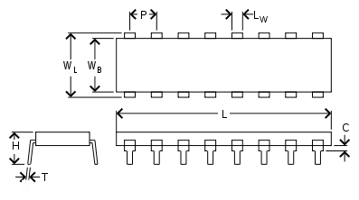
There are often subtle variations in package details from manufacturer to manufacturer, and even though standard designations are used, designers need to confirm dimensions when laying out printed circuit boards.
Note: It is relatively common to find packages that contain other components than their designated ones, such as diodes or voltage regulators in transistor packages, etc.
Categories:
Chip carriers
Semiconductor packages
Electronics lists
Hidden categories:
CS1 maint: archived copy as title
Webarchive template wayback links
Wikipedia articles needing clarification from July 2018


