Analog-to-digital converter


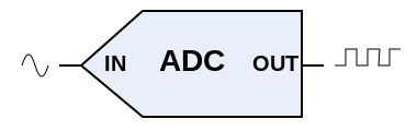
In electronics, an analog-to-digital converter (ADC, A/D, or A-to-D) is a system that converts an analog signal, such as a sound picked up by a microphone or light entering a digital camera, into a digital signal. An ADC may also provide an isolated measurement such as an electronic device that converts an input analog voltage or current to a digital number representing the magnitude of the voltage or current. Typically the digital output is a two's complement binary number that is proportional to the input, but there are other possibilities.
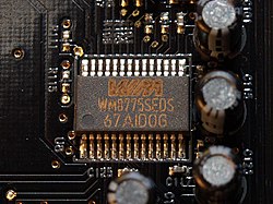
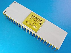
There are several ADC architectures. Due to the complexity and the need for precisely matched components, all but the most specialized ADCs are implemented as integrated circuits (ICs). These typically take the form of metal–oxide–semiconductor (MOS) mixed-signal integrated circuit chips that integrate both analog and digital circuits.
A digital-to-analog converter (DAC) performs the reverse function; it converts a digital signal into an analog signal.
Explanation[]
An ADC converts a continuous-time and continuous-amplitude analog signal to a discrete-time and discrete-amplitude digital signal. The conversion involves quantization of the input, so it necessarily introduces a small amount of error or noise. Furthermore, instead of continuously performing the conversion, an ADC does the conversion periodically, sampling the input, limiting the allowable bandwidth of the input signal.
The performance of an ADC is primarily characterized by its bandwidth and signal-to-noise ratio (SNR). The bandwidth of an ADC is characterized primarily by its sampling rate. The SNR of an ADC is influenced by many factors, including the resolution, linearity and accuracy (how well the quantization levels match the true analog signal), aliasing and jitter. The SNR of an ADC is often summarized in terms of its effective number of bits (ENOB), the number of bits of each measure it returns that are on average not noise. An ideal ADC has an ENOB equal to its resolution. ADCs are chosen to match the bandwidth and required SNR of the signal to be digitized. If an ADC operates at a sampling rate greater than twice the bandwidth of the signal, then per the Nyquist–Shannon sampling theorem, perfect reconstruction is possible. The presence of quantization error limits the SNR of even an ideal ADC. However, if the SNR of the ADC exceeds that of the input signal, its effects may be neglected resulting in an essentially perfect digital representation of the analog input signal.
Resolution[]

The resolution of the converter indicates the number of different, ie discrete, values it can produce over the allowed range of analog input values. Thus a particular resolution determines the magnitude of the quantization error and therefore determines the maximum possible signal-to-noise ratio for an ideal ADC without the use of oversampling. The input samples are usually stored electronically in binary form within the ADC, so the resolution is usually expressed as the audio bit depth. In consequence, the number of discrete values available is usually a power of two. For example, an ADC with a resolution of 8 bits can encode an analog input to one in 256 different levels (28 = 256). The values can represent the ranges from 0 to 255 (i.e. as unsigned integers) or from −128 to 127 (i.e. as signed integer), depending on the application.
Resolution can also be defined electrically, and expressed in volts. The change in voltage required to guarantee a change in the output code level is called the least significant bit (LSB) voltage. The resolution Q of the ADC is equal to the LSB voltage. The voltage resolution of an ADC is equal to its overall voltage measurement range divided by the number of intervals:

where M is the ADC's resolution in bits and EFSR is the full scale voltage range (also called 'span'). EFSR is given by

where VRefHi and VRefLow are the upper and lower extremes, respectively, of the voltages that can be coded.
Normally, the number of voltage intervals is given by

where M is the ADC's resolution in bits.[1]
That is, one voltage interval is assigned in between two consecutive code levels.
Example:
- Coding scheme as in figure 1
- Full scale measurement range = 0 to 1 volt
- ADC resolution is 3 bits: 23 = 8 quantization levels (codes)
- ADC voltage resolution, Q = 1 V / 8 = 0.125 V.
In many cases, the useful resolution of a converter is limited by the signal-to-noise ratio (SNR) and other errors in the overall system expressed as an ENOB.
Quantization error[]

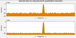
Quantization error is introduced by the quantization inherent in an ideal ADC. It is a rounding error between the analog input voltage to the ADC and the output digitized value. The error is nonlinear and signal-dependent. In an ideal ADC, where the quantization error is uniformly distributed between −1/2 LSB and +1/2 LSB, and the signal has a uniform distribution covering all quantization levels, the Signal-to-quantization-noise ratio (SQNR) is given by

where Q is the number of quantization bits. For example, for a 16-bit ADC, the quantization error is 96.3 dB below the maximum level.
Quantization error is distributed from DC to the Nyquist frequency. Consequently, if part of the ADC's bandwidth is not used, as is the case with oversampling, some of the quantization error will occur out-of-band, effectively improving the SQNR for the bandwidth in use. In an oversampled system, noise shaping can be used to further increase SQNR by forcing more quantization error out of band.
Dither[]
In ADCs, performance can usually be improved using dither. This is a very small amount of random noise (e.g. white noise), which is added to the input before conversion. Its effect is to randomize the state of the LSB based on the signal. Rather than the signal simply getting cut off altogether at low levels, it extends the effective range of signals that the ADC can convert, at the expense of a slight increase in noise. Note that dither can only increase the resolution of a sampler. It cannot improve the linearity, and thus accuracy does not necessarily improve.
Quantization distortion in an audio signal of very low level with respect to the bit depth of the ADC is correlated with the signal and sounds distorted and unpleasant. With dithering, the distortion is transformed into noise. The undistorted signal may be recovered accurately by averaging over time. Dithering is also used in integrating systems such as electricity meters. Since the values are added together, the dithering produces results that are more exact than the LSB of the analog-to-digital converter.
Dither is often applied when quantizing photographic images to a fewer number of bits per pixel—the image becomes noisier but to the eye looks far more realistic than the quantized image, which otherwise becomes banded. This analogous process may help to visualize the effect of dither on an analog audio signal that is converted to digital.
Accuracy[]
An ADC has several sources of errors. Quantization error and (assuming the ADC is intended to be linear) non-linearity are intrinsic to any analog-to-digital conversion. These errors are measured in a unit called the least significant bit (LSB). In the above example of an eight-bit ADC, an error of one LSB is 1/256 of the full signal range, or about 0.4%.
Nonlinearity[]
All ADCs suffer from nonlinearity errors caused by their physical imperfections, causing their output to deviate from a linear function (or some other function, in the case of a deliberately nonlinear ADC) of their input. These errors can sometimes be mitigated by calibration, or prevented by testing. Important parameters for linearity are integral nonlinearity and differential nonlinearity. These nonlinearities introduce distortion that can reduce the signal-to-noise ratio performance of the ADC and thus reduce its effective resolution.
Jitter[]
When digitizing a sine wave , the use of a non-ideal sampling clock will result in some uncertainty in when samples are recorded. Provided that the actual sampling time uncertainty due to clock jitter is , the error caused by this phenomenon can be estimated as . This will result in additional recorded noise that will reduce the effective number of bits (ENOB) below that predicted by quantization error alone. The error is zero for DC, small at low frequencies, but significant with signals of high amplitude and high frequency. The effect of jitter on performance can be compared to quantization error: , where q is the number of ADC bits.[citation needed]


| Output size (bits) |
Signal Frequency | ||||||
|---|---|---|---|---|---|---|---|
| 1 Hz | 1 kHz | 10 kHz | 1 MHz | 10 MHz | 100 MHz | 1 GHz | |
| 8 | 1,243 µs | 1.24 µs | 124 ns | 1.24 ns | 124 ps | 12.4 ps | 1.24 ps |
| 10 | 311 µs | 311 ns | 31.1 ns | 311 ps | 31.1 ps | 3.11 ps | 0.31 ps |
| 12 | 77.7 µs | 77.7 ns | 7.77 ns | 77.7 ps | 7.77 ps | 0.78 ps | 0.08 ps ("77.7fs") |
| 14 | 19.4 µs | 19.4 ns | 1.94 ns | 19.4 ps | 1.94 ps | 0.19 ps | 0.02 ps ("19.4fs") |
| 16 | 4.86 µs | 4.86 ns | 486 ps | 4.86 ps | 0.49 ps | 0.05 ps ("48.5 fs") | – |
| 18 | 1.21 µs | 1.21 ns | 121 ps | 1.21 ps | 0.12 ps | – | – |
| 20 | 304 ns | 304 ps | 30.4 ps | 0.30 ps ("303.56 fs") | 0.03 ps ("30.3 fs") | – | – |
| 24 | 18.9 ns | 18.9 ps | 1.89 ps | 0.019 ps ("18.9 fs") | - | – | – |
Clock jitter is caused by phase noise.[3][4] The resolution of ADCs with a digitization bandwidth between 1 MHz and 1 GHz is limited by jitter.[5] For lower bandwidth conversions such as when sampling audio signals at 44.1 kHz, clock jitter has a less significant impact on performance.[6]
Sampling rate[]
An analog signal is continuous in time and it is necessary to convert this to a flow of digital values. It is therefore required to define the rate at which new digital values are sampled from the analog signal. The rate of new values is called the sampling rate or sampling frequency of the converter. A continuously varying bandlimited signal can be sampled and then the original signal can be reproduced from the discrete-time values by a reconstruction filter. The Nyquist–Shannon sampling theorem implies that a faithful reproduction of the original signal is only possible if the sampling rate is higher than twice the highest frequency of the signal.
Since a practical ADC cannot make an instantaneous conversion, the input value must necessarily be held constant during the time that the converter performs a conversion (called the conversion time). An input circuit called a sample and hold performs this task—in most cases by using a capacitor to store the analog voltage at the input, and using an electronic switch or gate to disconnect the capacitor from the input. Many ADC integrated circuits include the sample and hold subsystem internally.
Aliasing[]
An ADC works by sampling the value of the input at discrete intervals in time. Provided that the input is sampled above the Nyquist rate, defined as twice the highest frequency of interest, then all frequencies in the signal can be reconstructed. If frequencies above half the Nyquist rate are sampled, they are incorrectly detected as lower frequencies, a process referred to as aliasing. Aliasing occurs because instantaneously sampling a function at two or fewer times per cycle results in missed cycles, and therefore the appearance of an incorrectly lower frequency. For example, a 2 kHz sine wave being sampled at 1.5 kHz would be reconstructed as a 500 Hz sine wave.
To avoid aliasing, the input to an ADC must be low-pass filtered to remove frequencies above half the sampling rate. This filter is called an anti-aliasing filter, and is essential for a practical ADC system that is applied to analog signals with higher frequency content. In applications where protection against aliasing is essential, oversampling may be used to greatly reduce or even eliminate it.
Although aliasing in most systems is unwanted, it can be exploited to provide simultaneous down-mixing of a band-limited high-frequency signal (see undersampling and frequency mixer). The alias is effectively the lower heterodyne of the signal frequency and sampling frequency.[7]
Oversampling[]
For economy, signals are often sampled at the minimum rate required with the result that the quantization error introduced is white noise spread over the whole passband of the converter. If a signal is sampled at a rate much higher than the Nyquist rate and then digitally filtered to limit it to the signal bandwidth produces the following advantages:
- Oversampling can make it easier to realize analog anti-aliasing filters
- Improved audio bit depth
- Reduced noise, especially when noise shaping is employed in addition to oversampling.
Oversampling is typically used in audio frequency ADCs where the required sampling rate (typically 44.1 or 48 kHz) is very low compared to the clock speed of typical transistor circuits (>1 MHz). In this case, the performance of the ADC can be greatly increased at little or no cost. Furthermore, as any aliased signals are also typically out of band, aliasing can often be completely eliminated using very low cost filters.
Relative speed and precision[]
The speed of an ADC varies by type. The Wilkinson ADC is limited by the clock rate which is processable by current digital circuits. For a successive-approximation ADC, the conversion time scales with the logarithm of the resolution, i.e. the number of bits. Flash ADCs are certainly the fastest type of the three; The conversion is basically performed in a single parallel step.
There is a potential tradeoff between speed and precision. Flash ADCs have drifts and uncertainties associated with the comparator levels results in poor linearity. To a lesser extent, poor linearity can also be an issue for successive-approximation ADCs. Here, nonlinearity arises from accumulating errors from the subtraction processes. Wilkinson ADCs have the best linearity of the three.[8][9]
Sliding scale principle[]
The sliding scale or randomizing method can be employed to greatly improve the linearity of any type of ADC, but especially flash and successive approximation types. For any ADC the mapping from input voltage to digital output value is not exactly a floor or ceiling function as it should be. Under normal conditions, a pulse of a particular amplitude is always converted to the same digital value. The problem lies in that the ranges of analog values for the digitized values are not all of the same widths, and the differential linearity decreases proportionally with the divergence from the average width. The sliding scale principle uses an averaging effect to overcome this phenomenon. A random, but known analog voltage is added to the sampled input voltage. It is then converted to digital form, and the equivalent digital amount is subtracted, thus restoring it to its original value. The advantage is that the conversion has taken place at a random point. The statistical distribution of the final levels is decided by a weighted average over a region of the range of the ADC. This in turn desensitizes it to the width of any specific level.[10][11]
Types[]
These are several common ways of implementing an electronic ADC.
Direct-conversion[]
A direct-conversion or flash ADC has a bank of comparators sampling the input signal in parallel, each firing for a specific voltage range. The comparator bank feeds a logic circuit that generates a code for each voltage range.
ADCs of this type have a large die size and high power dissipation. They are often used for video, wideband communications, or other fast signals in optical and magnetic storage.
The circuit consists of a resistive divider network, a set of op-amp comparators and a priority encoder. A small amount of hysteresis is built into the comparator to resolve any problems at voltage boundaries. At each node of the resistive divider, a comparison voltage is available. The purpose of the circuit is to compare the analog input voltage with each of the node voltages.
The circuit has the advantage of high speed as the conversion takes place simultaneously rather than sequentially. Typical conversion time is 100 ns or less. Conversion time is limited only by the speed of the comparator and of the priority encoder. This type of ADC has the disadvantage that the number of comparators required almost doubles for each added bit. Also, the larger the value of n, the more complex is the priority encoder.
Successive approximation[]
A successive-approximation ADC uses a comparator and a binary search to successively narrow a range that contains the input voltage. At each successive step, the converter compares the input voltage to the output of an internal digital to analog converter which initially represents the midpoint of the allowed input voltage range. At each step in this process, the approximation is stored in a successive approximation register (SAR) and the output of the digital to analog converter is updated for a comparison over a narrower range.
Ramp-compare[]
A ramp-compare ADC produces a saw-tooth signal that ramps up or down then quickly returns to zero. When the ramp starts, a timer starts counting. When the ramp voltage matches the input, a comparator fires, and the timer's value is recorded. Timed ramp converters can be implemented economically,[a] however, the ramp time may be sensitive to temperature because the circuit generating the ramp is often a simple analog integrator. A more accurate converter uses a clocked counter driving a DAC. A special advantage of the ramp-compare system is that converting a second signal just requires another comparator and another register to store the timer value. To reduce sensitivity to input changes during conversion, a sample and hold can charge a capacitor with the instantaneous input voltage and the converter can time the time required to discharge with a constant current.
Wilkinson[]
The Wilkinson ADC was designed by Denys Wilkinson in 1950. The Wilkinson ADC is based on the comparison of an input voltage with that produced by a charging capacitor. The capacitor is allowed to charge until a comparator determines it matches the input voltage. Then, the capacitor is discharged linearly. The time required to discharge the capacitor is proportional to the amplitude of the input voltage. While the capacitor is discharging, pulses from a high-frequency oscillator clock are counted by a register. The number of clock pulses recorded in the register is also proportional to the input voltage.[13][14]
Integrating[]
An integrating ADC (also dual-slope or multi-slope ADC) applies the unknown input voltage to the input of an integrator and allows the voltage to ramp for a fixed time period (the run-up period). Then a known reference voltage of opposite polarity is applied to the integrator and is allowed to ramp until the integrator output returns to zero (the run-down period). The input voltage is computed as a function of the reference voltage, the constant run-up time period, and the measured run-down time period. The run-down time measurement is usually made in units of the converter's clock, so longer integration times allow for higher resolutions. Likewise, the speed of the converter can be improved by sacrificing resolution. Converters of this type (or variations on the concept) are used in most for their linearity and flexibility.
- Charge balancing ADC
- The principle of charge balancing ADC is to first convert the input signal to a frequency using a voltage-to-frequency converter. This frequency is then measured by a counter and converted to an output code proportional to the analog input. The main advantage of these converters is that it is possible to transmit frequency even in a noisy environment or in isolated form. However, the limitation of this circuit is that the output of the voltage-to-frequency converter depends upon an RC product whose value cannot be accurately maintained over temperature and time.
- Dual-slope ADC
- The analog part of the circuit consists of a high input impedance buffer, precision integrator and a voltage comparator. The converter first integrates the analog input signal for a fixed duration and then it integrates an internal reference voltage of opposite polarity until the integrator output is zero. The main disadvantage of this circuit is the long duration time. They are particularly suitable for accurate measurement of slowly varying signals such as thermocouples and weighing scales.
Delta-encoded[]
A delta-encoded or counter-ramp ADC has an up-down counter that feeds a digital to analog converter (DAC). The input signal and the DAC both go to a comparator. The comparator controls the counter. The circuit uses negative feedback from the comparator to adjust the counter until the DAC's output matches the input signal and number is read from the counter. Delta converters have very wide ranges and high resolution, but the conversion time is dependent on the input signal behavior, though it will always have a guaranteed worst-case. Delta converters are often very good choices to read real-world signals as most signals from physical systems do not change abruptly. Some converters combine the delta and successive approximation approaches; this works especially well when high frequency components of the input signal are known to be small in magnitude.
Pipelined[]
A pipelined ADC (also called subranging quantizer) uses two or more conversion steps. First, a coarse conversion is done. In a second step, the difference to the input signal is determined with a digital to analog converter (DAC). This difference is then converted more precisely, and the results are combined in the last step. This can be considered a refinement of the successive-approximation ADC wherein the feedback reference signal consists of the interim conversion of a whole range of bits (for example, four bits) rather than just the next-most-significant bit. By combining the merits of the successive approximation and flash ADCs this type is fast, has a high resolution, and can be implemented efficiently.
Sigma-delta[]
A sigma-delta ADC (also known as a delta-sigma ADC) oversamples the incoming signal by a large factor using a smaller number of bits than required are converted using a flash ADC and filters the desired signal band. The resulting signal, along with the error generated by the discrete levels of the flash, is fed back and subtracted from the input to the filter. This negative feedback has the effect of noise shaping the quantization error that it does not appear in the desired signal frequencies. A digital filter (decimation filter) follows the ADC which reduces the sampling rate, filters off unwanted noise signal and increases the resolution of the output.
Time-interleaved[]
A time-interleaved ADC uses M parallel ADCs where each ADC samples data every M:th cycle of the effective sample clock. The result is that the sample rate is increased M times compared to what each individual ADC can manage. In practice, the individual differences between the M ADCs degrade the overall performance reducing the spurious-free dynamic range (SFDR).[15] However, technologies exist to correct for these time-interleaving mismatch errors.
Intermediate FM stage[]
An ADC with intermediate FM stage first uses a voltage-to-frequency converter to convert the desired signal into an oscillating signal with a frequency proportional to the voltage of the desired signal, and then uses a frequency counter to convert that frequency into a digital count proportional to the desired signal voltage. Longer integration times allow for higher resolutions. Likewise, the speed of the converter can be improved by sacrificing resolution. The two parts of the ADC may be widely separated, with the frequency signal passed through an opto-isolator or transmitted wirelessly. Some such ADCs use sine wave or square wave frequency modulation; others use pulse-frequency modulation. Such ADCs were once the most popular way to show a digital display of the status of a remote analog sensor.[16][17][18][19][20]
Other types[]
There can be other ADCs that use a combination of electronics and other technologies. A time-stretch analog-to-digital converter (TS-ADC) digitizes a very wide bandwidth analog signal, that cannot be digitized by a conventional electronic ADC, by time-stretching the signal prior to digitization. It commonly uses a photonic preprocessor frontend to time-stretch the signal, which effectively slows the signal down in time and compresses its bandwidth. As a result, an electronic backend ADC, that would have been too slow to capture the original signal, can now capture this slowed down signal. For continuous capture of the signal, the frontend also divides the signal into multiple segments in addition to time-stretching. Each segment is individually digitized by a separate electronic ADC. Finally, a digital signal processor rearranges the samples and removes any distortions added by the frontend to yield the binary data that is the digital representation of the original analog signal.
Commercial[]
This section does not cite any sources. (July 2018) |
Commercial ADCs are usually implemented as integrated circuits. Most converters sample with 6 to 24 bits of resolution, and produce fewer than 1 megasample per second. Thermal noise generated by passive components such as resistors masks the measurement when higher resolution is desired. For audio applications and in-room temperatures, such noise is usually a little less than 1 μV (microvolt) of white noise. If the MSB corresponds to a standard 2 V of output signal, this translates to a noise-limited performance that is less than 20~21 bits, and removes the need for any dithering. Mega-sample converters are required in digital video cameras, video capture cards, and TV tuner cards to convert full-speed analog video to digital video files.
In many cases, the most expensive part of an integrated circuit is the pins, because they make the package larger, and each pin has to be connected to the integrated circuit's silicon. To save pins, it is common for ADCs to send their data one bit at a time over a serial interface to the computer, with the next bit coming out when a clock signal changes state. This saves quite a few pins on the ADC package, and in many cases, does not make the overall design any more complex (even microprocessors which use memory-mapped I/O only need a few bits of a port to implement a serial bus to an ADC).
Commercial ADCs often have several inputs that feed the same converter, usually through an analog multiplexer. Different models of ADC may include sample and hold circuits, instrumentation amplifiers or differential inputs, where the quantity measured is the difference between two voltages.
Applications[]
Music recording[]
Analog-to-digital converters are integral to 2000s era music reproduction technology and digital audio workstation-based sound recording. People often produce music on computers using an analog recording and therefore need analog-to-digital converters to create the pulse-code modulation (PCM) data streams that go onto compact discs and digital music files. The current crop of analog-to-digital converters utilized in music can sample at rates up to 192 kilohertz. Considerable literature exists on these matters, but commercial considerations often play a significant role. Many recording studios record in 24-bit/96 kHz (or higher) pulse-code modulation (PCM) or Direct Stream Digital (DSD) formats, and then downsample or decimate the signal for Compact Disc Digital Audio production (44.1 kHz) or to 48 kHz for commonly used radio and television broadcast applications because of the Nyquist frequency and hearing range of humans.
Digital signal processing[]
ADCs are required to process, store, or transport virtually any analog signal in digital form. TV tuner cards, for example, use fast video analog-to-digital converters. Slow on-chip 8, 10, 12, or 16 bit analog-to-digital converters are common in microcontrollers. Digital storage oscilloscopes need very fast analog-to-digital converters, also crucial for software defined radio and their new applications.
Scientific instruments[]
Digital imaging systems commonly use analog-to-digital converters in digitizing pixels. Some radar systems commonly use analog-to-digital converters to convert signal strength to digital values for subsequent signal processing. Many other in situ and remote sensing systems commonly use analogous technology. The number of binary bits in the resulting digitized numeric values reflects the resolution, the number of unique discrete levels of quantization (signal processing). The correspondence between the analog signal and the digital signal depends on the quantization error. The quantization process must occur at an adequate speed, a constraint that may limit the resolution of the digital signal. Many sensors in scientific instruments produce an analog signal; temperature, pressure, pH, light intensity etc. All these signals can be amplified and fed to an ADC to produce a digital number proportional to the input signal.
Rotary encoder[]
Some non-electronic or only partially electronic devices, such as rotary encoders, can also be considered ADCs. Typically the digital output of an ADC will be a two's complement binary number that is proportional to the input. An encoder might output a Gray code.
Displaying[]
Flat panel displays are inherently digital and need an ADC to process an analog signal such as composite or VGA.
Electrical symbol[]
Testing[]
Testing an Analog to Digital Converter requires an analog input source and hardware to send control signals and capture digital data output. Some ADCs also require an accurate source of reference signal.
The key parameters to test an ADC are:
- DC offset error
- DC gain error
- Signal to noise ratio (SNR)
- Total harmonic distortion (THD)
- Integral nonlinearity (INL)
- Differential nonlinearity (DNL)
- Spurious free dynamic range
- Power dissipation
See also[]
- Adaptive predictive coding, a type of ADC in which the value of the signal is predicted by a linear function
- Audio codec
- Beta encoder
- Digitization
- Digital signal processing
- Integral linearity
- Modem
Notes[]
References[]
- ^ "Principles of Data Acquisition and Conversion" (PDF). Texas Instruments. April 2015. Retrieved 2016-10-18.
- ^ Lathi, B.P. (1998). Modern Digital and Analog Communication Systems (3rd ed.). Oxford University Press.
- ^ "Maxim App 800: Design a Low-Jitter Clock for High-Speed Data Converters", maxim-ic.com, July 17, 2002
- ^ "Jitter effects on Analog to Digital and Digital to Analog Converters" (PDF). Retrieved 19 August 2012.
- ^ Löhning, Michael; Fettweis, Gerhard (2007). "The effects of aperture jitter and clock jitter in wideband ADCs". Computer Standards & Interfaces Archive. 29 (1): 11–18. CiteSeerX 10.1.1.3.9217. doi:10.1016/j.csi.2005.12.005.
- ^ Redmayne, Derek; Steer, Alison (8 December 2008), "Understanding the effect of clock jitter on high-speed ADCs", eetimes.com
- ^ "RF-Sampling and GSPS ADCs – Breakthrough ADCs Revolutionize Radio Architectures" (PDF). Texas Instruments. Retrieved 4 November 2013.
- ^ Knoll (1989, pp. 664–665)
- ^ Nicholson (1974, pp. 313–315)
- ^ Knoll (1989, pp. 665–666)
- ^ Nicholson (1974, pp. 315–316)
- ^ "Atmel Application Note AVR400: Low Cost A/D Converter" (PDF). atmel.com.
- ^ Knoll (1989, pp. 663–664)
- ^ Nicholson (1974, pp. 309–310)
- ^ Vogel, Christian (2005). "The Impact of Combined Channel Mismatch Effects in Time-interleaved ADCs" (PDF). IEEE Transactions on Instrumentation and Measurement. 55 (1): 415–427. CiteSeerX 10.1.1.212.7539. doi:10.1109/TIM.2004.834046. S2CID 15038020.
- ^ Analog Devices MT-028 Tutorial: "Voltage-to-Frequency Converters" by Walt Kester and James Bryant 2009, apparently adapted from Kester, Walter Allan (2005) Data conversion handbook, Newnes, p. 274, ISBN 0750678410.
- ^ Microchip AN795 "Voltage to Frequency / Frequency to Voltage Converter" p. 4: "13-bit A/D converter"
- ^ Carr, Joseph J. (1996) Elements of electronic instrumentation and measurement, Prentice Hall, p. 402, ISBN 0133416860.
- ^ "Voltage-to-Frequency Analog-to-Digital Converters". globalspec.com
- ^ Pease, Robert A. (1991) Troubleshooting Analog Circuits, Newnes, p. 130, ISBN 0750694998.
- Knoll, Glenn F. (1989). Radiation Detection and Measurement (2nd ed.). New York: John Wiley & Sons. ISBN 978-0471815044.
- Nicholson, P. W. (1974). Nuclear Electronics. New York: John Wiley & Sons. pp. 315–316. ISBN 978-0471636977.
Further reading[]
- Allen, Phillip E.; Holberg, Douglas R. (2002). CMOS Analog Circuit Design. ISBN 978-0-19-511644-1.
- Fraden, Jacob (2010). Handbook of Modern Sensors: Physics, Designs, and Applications. Springer. ISBN 978-1441964656.
- Kester, Walt, ed. (2005). The Data Conversion Handbook. Elsevier: Newnes. ISBN 978-0-7506-7841-4.
- Johns, David; Martin, Ken (1997). Analog Integrated Circuit Design. ISBN 978-0-471-14448-9.
- Liu, Mingliang (2006). Demystifying Switched-Capacitor Circuits. ISBN 978-0-7506-7907-7.
- Norsworthy, Steven R.; Schreier, Richard; Temes, Gabor C. (1997). Delta-Sigma Data Converters. IEEE Press. ISBN 978-0-7803-1045-2.
- Razavi, Behzad (1995). Principles of Data Conversion System Design. New York, NY: IEEE Press. ISBN 978-0-7803-1093-3.
- Ndjountche, Tertulien (24 May 2011). CMOS Analog Integrated Circuits: High-Speed and Power-Efficient Design. Boca Raton, FL: CRC Press. ISBN 978-1-4398-5491-4.
- Staller, Len (February 24, 2005). "Understanding analog to digital converter specifications". Embedded Systems Design.
- Walden, R. H. (1999). "Analog-to-digital converter survey and analysis". IEEE Journal on Selected Areas in Communications. 17 (4): 539–550. CiteSeerX 10.1.1.352.1881. doi:10.1109/49.761034.
External links[]
| Wikibooks has a book on the topic of: Analog and Digital Conversion |
- An Introduction to Delta Sigma Converters A very nice overview of Delta-Sigma converter theory.
- Digital Dynamic Analysis of A/D Conversion Systems through Evaluation Software based on FFT/DFT Analysis RF Expo East, 1987
- Which ADC Architecture Is Right for Your Application? article by Walt Kester
- ADC and DAC Glossary Defines commonly used technical terms.
- Introduction to ADC in AVR – Analog to digital conversion with Atmel microcontrollers
- Signal processing and system aspects of time-interleaved ADCs.
- Explanation of analog-digital converters with interactive principles of operations.
- MATLAB Simulink model of a simple ramp ADC.
| show Authority control |
|---|
- Digital signal processing
- Electronic circuits