Mixed-signal integrated circuit
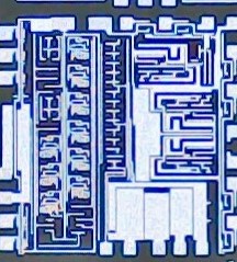
A mixed-signal integrated circuit is any integrated circuit that has both analog circuits and digital circuits on a single semiconductor die.[1][2][3][4]
In real-life applications mixed-signal designs are everywhere, for example, in smart mobile phones, sensor systems with on-chip standardized digital interfaces (like I2C, UART, SPI, CAN etc.),voice related signal processing, aerospace and space electronics, IoT, unmanned aerial vehicles (UAVs), automotive and other electrical vehicles. Mixed-signal ICs also process both analog and digital signals together. For example, an analog-to-digital converter (ADC) is a typical mixed-signal circuit. Mixed-signal circuits or systems are typically cost-effective solutions for building any modern consumer electronics, industrial, medical, measurement, space etc. applications. A mixed signal integrated circuit may also contain on-chip memory blocks like OTP, which complicates the manufacturing compared to analog ICs. A mixed signal integrated circuit minimizes off-chip interconnects between digital and analog functionality in the system, typically size and weight of the realization due to minimized packaging and reduced system board (PWB/PCB, module substrate etc.) size and therefore increase the reliability of the system.
Mixed signal devices are available as standard parts, but custom designed application-specific integrated circuits (ASICs) are designed for new applications or if new standards are emerging or new energy source(s) are implemented in the system and the production volumes are estimated to be high. Availability of ready and tested analog and mixed signal IP blocks from foundries or dedicated design houses have lowered the gap to realize mixed signal ASICs. There also exists few mixed signal FPGAs and microcontrollers, which typically may include analog-to-digital and digital-to-analog converter(s), operational amplifiers, even wireless connectivity blocks etc. on the same chip with digital logic. [5] Mixed signal FPGAs are an extension of field-programmable analog arrays. These mixed signal FPGAs and microcontrollers are bridging the gap between standard mixed signal devices, full custom ASICs and possibly embedded software world, when products are under development or the volumes are too low for an effective full custom ASIC realization. However there can be few performance limitations typically with these type of FPGAs and microcontrollers like resolution of ADCs, speed of digital to analog conversion (DAC) and limited number of inputs and outputs etc. Despite these possible limitations mixed signal FPGAs and microcontrollers can speed up the system architecture design, prototyping and even small and medium scale production. They also can be backed-up with development boards, development community and possibly also software support.
Introduction[]
An analog-mixed-signal system-on-a-chip (AMS-SoC) can be a combination of analog circuits, digital circuits, intrinsic mixed-signal circuits (like ADCs), and in some cases possibly also embedded software.
Integrated circuits (ICs) are generally classified as digital (e.g. a microprocessor) or analog (e.g. an operational amplifier). Mixed-signal ICs are chips that contain both digital and analog circuitry on the same chip. This category of chip has grown in volumes dramatically specifically with the increased use of 3G, 4G, 5G etc. cell phones and other portable technologies as well as increase of sensors and electronics in automotives.
Mixed-signal ICs are often used to convert analog signals to digital signals so that digital devices can process them. For example, mixed-signal ICs are essential components for FM tuners in digital products such as media players, which have digital amplifiers. Any analog signal (such as an FM radio transmission, a light wave or a sound) can be digitized using a very basic analog-to-digital converter, and the smallest and most energy efficient of these would be in the form of mixed-signal ICs.
Mixed-signal ICs are more difficult to design and manufacture than analog-only or digital-only integrated circuits. For example, an efficient mixed-signal IC would have its digital and analog components share a common power supply. However, analog and digital components have very different power needs and consumption characteristics that make this a non-trivial goal in chip design.
Realization of mixed-signal functionality requires from manufacturing technologies additionally to traditional active (various transistors) also options and modelling understanding to realize well performing passive elements like coils, capacitors and resistors on the same chip with digital functionality. High voltage transistors might be needed in the power management functions on the same chip with digital functionality possibly with a low power CMOS processor system. Some advanced mixed signal technologies may enable even analog sensor elements like pressure sensors or imaging diodes on the same chip with analog digital converter. Typically mixed-signal ICs are not necessarily needing fastest digital performance but need more mature models of active and passive elements for more accurate simulations and verification like for testability planning and reliability estimations. Therefore mixed-signal circuits are typically realized with larger line widths than highest speed and most dense digital logic, and the implementation technologies can be 2-4 nodes behind the latest digital implementation technologies. Additionally mixed signal processing may need passive elements like resistors, capacitors and coils, which may require specific metal or dielectric layers or similar. Because of these specific requirements the manufacturers of mixed signal devices foundries can be different from the digital IC manufacturers or foundries.
Examples[]
Typically, mixed-signal chips perform some whole function or sub-function in a larger assembly such as the radio subsystem of a cell phone, or the read data path and laser sled control logic of a DVD player. They often contain an entire system-on-a-chip.
Examples of mixed-signal integrated circuits include data converters using delta-sigma modulation, analog-to-digital converter/digital-to-analog converter using error detection and correction, and digital radio chips. Digitally controlled sound chips are also mixed-signal circuits. With the advent of cellular technology and network technology this category now includes cellular telephone, software radio, LAN and WAN router integrated circuits.
Because of the use of both digital signal processing and analog circuitry, mixed-signal ICs are usually designed for a very specific purpose and their design requires a high level of expertise and careful use of computer aided design (CAD) tools. There also exists specific design tools like mixed signal simulators or description languages like VHDL-AMS. Automated testing of the finished chips can also be challenging. Teradyne, Keysight,[6] and Advantest are the major suppliers of the test equipment for mixed-signal chips.
The particular challenges of mixed signal include:
- CMOS technology is usually optimal for digital performance and scaling while bipolar transistors are usually optimal for analog performance, yet until the last decade it has been difficult to either combine these cost-effectively or to design both analog and digital in a single technology without serious performance compromises. The advent of technologies like high performance CMOS, BiCMOS, CMOS SOI and SiGe have removed many of the compromises that previously had to be made.
- Testing functional operation of mixed-signal ICs remains complex, expensive and often a "one-off" implementation task.
- Systematic design methodologies comparable to digital design methods are far more primitive in the analog and mixed-signal arena. Analog circuit design can not generally be automated to nearly the extent that digital circuit design can. Combining the two technologies multiplies this complication.
- Fast-changing digital signals send noise to sensitive analog inputs. One path for this noise is substrate coupling. A variety of techniques are used to attempt to block or cancel this noise coupling, such as fully differential amplifiers,[7] P+ guard-rings,[8] differential topology, on-chip decoupling, and triple-well isolation.[9]
Most modern radio and telecommunications use mixed-signal circuits.
Commercial examples[]
- Few examples of mixed signal design houses/resources (there are various sources):
- Examples of mixed signal FPGAs and microcontrollers:
- Analog Devices CM4xx Mixed-Signal Control Processors
- Fusion FPGA (from Microsemi now part of Microchip Technology)
- PSoC PSoC Programmable System on Chip, product from Infineon Technologies (former Cypress Semiconductor)
- Texas Instruments' MSP430
- Xilinx mixed signal FPGA
- Examples of mixed signal foundries. Some foundries may also have design service or list of partners capable for mixed signal design services for their technologies:
- Globalfoundries
- New Japan Radio
- Tower Semiconductor Ltd
- X-Fab
- List of sound chips
- Yamaha FM synthesis sound chips
- Atari POKEY
- MOS Technology SID
History[]
MOS switched-capacitor circuits[]
The metal–oxide–semiconductor field-effect transistor (MOSFET, or MOS transistor) was invented by Mohamed M. Atalla and Dawon Kahng at Bell Telephone Laboratories in 1959, and the MOS integrated circuit (MOS IC) chip was proposed soon after, but MOS technology was initially overlooked by Bell because they did not find it practical for analog telephone applications, before it was commercialized by Fairchild and RCA for digital electronics such as computers.[10][11] MOS technology eventually became practical for telephony applications with the MOS mixed-signal integrated circuit, which combines analog and digital signal processing on a single chip, developed by former Bell engineer David A. Hodges with Paul R. Gray at UC Berkeley in the early 1970s.[11] In 1974, Hodges and Gray worked with R.E. Suarez to develop MOS switched capacitor (SC) circuit technology, which they used to develop a digital-to-analog converter (DAC) chip, using MOS capacitors and MOSFET switches for data conversion.[11] MOS analog-to-digital converter (ADC) and DAC chips were commercialized by 1974.[12]
MOS SC circuits led to the development of pulse-code modulation (PCM) codec-filter chips in the late 1970s.[11][13] The silicon-gate CMOS (complementary MOS) PCM codec-filter chip, developed by Hodges and W.C. Black in 1980,[11] has since been the industry standard for digital telephony.[11][13] By the 1990s, telecommunication networks such as the public switched telephone network (PSTN) had been largely digitized with very-large-scale integration (VLSI) CMOS PCM codec-filters, widely used in electronic switching systems for telephone exchanges, private branch exchanges (PBX) and key telephone systems (KTS); user-end modems; data transmission applications such as digital loop carriers, pair gain multiplexers, telephone loop extenders, integrated services digital network (ISDN) terminals, digital cordless telephones and digital cell phones; and applications such as speech recognition equipment, voice data storage, voice mail and digital tapeless answering machines.[13] The bandwidth of digital telecommunication networks has been rapidly increasing at an exponential rate, as observed by Edholm's law,[14] largely driven by the rapid scaling and miniaturization of MOS technology.[15][11]
RF CMOS circuits[]
While working at Bell Labs in the early 1980s, Pakistani engineer Asad Abidi worked on the development of sub-micron MOSFET (metal–oxide–semiconductor field-effect transistor) VLSI (very large-scale integration) technology at the Advanced LSI Development Lab, along with Marty Lepselter, George E. Smith and Harry Bol. As one of the few circuit designers at the lab, Abidi demonstrated the potential of sub-micron NMOS integrated circuit technology in high-speed communication circuits, and developed the first MOS amplifiers for Gb/s data rates in optical fiber receivers. Abidi's work was initially met with skepticism from proponents of GaAs and bipolar junction transistors, the dominant technologies for high-speed circuits at the time. In 1985 he joined UCLA, where he pioneered RF CMOS technology in the late 1980s. His work changed the way in which RF circuits would be designed, away from discrete bipolar transistors and towards CMOS integrated circuits.[16]
Abidi was researching analog CMOS circuits for signal processing and communications during the late 1980s to early 1990s. In the mid-1990s, the RF CMOS technology that he pioneered was widely adopted in wireless networking, as mobile phones began entering widespread use. As of 2008, the radio transceivers in all wireless networking devices and modern mobile phones are mass-produced as RF CMOS devices.[16]
The baseband processors[17][18] and radio transceivers in all modern wireless networking devices and mobile phones are mass-produced using RF CMOS devices.[16] RF CMOS circuits are widely used to transmit and receive wireless signals, in a variety of applications, such as satellite technology (such as GPS), bluetooth, Wi-Fi, near-field communication (NFC), mobile networks (such as 3G, 4G and 5G), terrestrial broadcast, and automotive radar applications, among other uses.[19] RF CMOS technology is crucial to modern wireless communications, including wireless networks and mobile communication devices.[20]
See also[]
- Analog front-end
- RFIC
- RF CMOS (used for RF circuits in wireless communications)
References[]
- ^ Saraju Mohanty, Nanoelectronic Mixed-Signal System Design, McGraw-Hill, 2015, ISBN 978-0071825719 and 0071825711.
- ^ "Mixed-Signal IC Design". quote: "mixed-signal (IC's with mixed analog and digital circuits on a single chip)"
- ^ Mark Burns and Gordon W. Roberts, "An Introduction to Mixed-Signal IC Test and Measurement", 2001.
- ^ "ESS Mixed Signal Circuits" Archived 2010-10-11 at the Wayback Machine
- ^ "Microsemi Fusion mixed-signal FPGA"
- ^ "Electronic design, test automation and measurement equipment". Keysight Technologies.
- ^ "Fully differential current-input CMOS amplifier front-endsuppressing mixed signal substrate noise for optoelectronic applications" by Chang, J.J.; Myunghee Lee; Sungyong Jung; Brooke, M.A.; Jokerst, N.M.; Wills, D.S. 1999
- ^ "Substrate noise issues in mixed-signal chip designs using Spice" by Singh, R.; Sali, S. 1997
- ^ "Mixed-Signal IC Merges 14-Bit ADC With DSP In 0.18-μm CMOS"
- ^ Maloberti, Franco; Davies, Anthony C. (2016). "History of Electronic Devices" (PDF). A Short History of Circuits and Systems: From Green, Mobile, Pervasive Networking to Big Data Computing. IEEE Circuits and Systems Society. pp. 59-70 (65-7). ISBN 9788793609860.
- ^ Jump up to: a b c d e f g Allstot, David J. (2016). "Switched Capacitor Filters" (PDF). In Maloberti, Franco; Davies, Anthony C. (eds.). A Short History of Circuits and Systems: From Green, Mobile, Pervasive Networking to Big Data Computing. IEEE Circuits and Systems Society. pp. 105–110. ISBN 9788793609860.
- ^ Electronic Components. U.S. Government Printing Office. 1974. p. 46.
- ^ Jump up to: a b c Floyd, Michael D.; Hillman, Garth D. (8 October 2018) [1st pub. 2000]. "Pulse-Code Modulation Codec-Filters". The Communications Handbook (2nd ed.). CRC Press. pp. 26–1, 26–2, 26–3.
- ^ Cherry, Steven (2004). "Edholm's law of bandwidth". IEEE Spectrum. 41 (7): 58–60. doi:10.1109/MSPEC.2004.1309810.
- ^ Jindal, Renuka P. (2009). "From millibits to terabits per second and beyond - Over 60 years of innovation". 2009 2nd International Workshop on Electron Devices and Semiconductor Technology: 1–6. doi:10.1109/EDST.2009.5166093. ISBN 978-1-4244-3831-0.
- ^ Jump up to: a b c O'Neill, A. (2008). "Asad Abidi Recognized for Work in RF-CMOS". IEEE Solid-State Circuits Society Newsletter. 13 (1): 57–58. doi:10.1109/N-SSC.2008.4785694. ISSN 1098-4232.
- ^ Chen, Wai-Kai (2018). The VLSI Handbook. CRC Press. pp. 60–2. ISBN 9781420005967.
- ^ Morgado, Alonso; Río, Rocío del; Rosa, José M. de la (2011). Nanometer CMOS Sigma-Delta Modulators for Software Defined Radio. Springer Science & Business Media. p. 1. ISBN 9781461400370.
- ^ Veendrick, Harry J. M. (2017). Nanometer CMOS ICs: From Basics to ASICs. Springer. p. 243. ISBN 9783319475974.
- ^ "Infineon Hits Bulk-CMOS RF Switch Milestone". EE Times. 20 November 2018. Retrieved 26 October 2019.
Further reading[]
- Saraju Mohanty (2015). Nanoelectronic Mixed-Signal System Design. McGraw-Hill. ISBN 978-0071825719.
- R. Jacob Baker (2009). CMOS Mixed-Signal Circuit Design, Second Edition. http://CMOSedu.com/
- Electronic design