Semiconductor device fabrication
| Semiconductor device fabrication |
|---|
 |
|
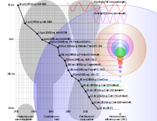
MOSFET scaling (process nodes) |
|

| External image | |
|---|---|
Semiconductor device fabrication is the process used to manufacture semiconductor devices, typically the metal–oxide–semiconductor (MOS) devices used in the integrated circuit (IC) chips such as modern computer processors, microcontrollers, and memory chips such as NAND flash and DRAM that are present in everyday electrical and electronic devices. It is a multiple-step sequence of photolithographic and chemical processing steps (such as surface passivation, thermal oxidation, planar diffusion and junction isolation) during which electronic circuits are gradually created on a wafer made of pure semiconducting material. Silicon is almost always used, but various compound semiconductors are used for specialized applications.
The entire manufacturing process, from start to packaged chips ready for shipment, takes six to eight weeks and is performed in highly specialized semiconductor fabrication plants, also called foundries or fabs.[1] All fabrication takes place inside a clean room, which is the central part of a fab. In more advanced semiconductor devices, such as modern 14/10/7 nm nodes, fabrication can take up to 15 weeks, with 11–13 weeks being the industry average.[2] Production in advanced fabrication facilities is completely automated and carried out in a hermetically sealed nitrogen environment to improve yield (the percent of microchips that function correctly in a wafer), with automated material handling systems taking care of the transport of wafers from machine to machine. Wafers are transported inside FOUPs, special sealed plastic boxes. All machinery and FOUPs contain an internal nitrogen atmosphere. The air inside the machinery and FOUPs is usually kept cleaner than the surrounding air in the cleanroom. This internal atmosphere is known as a mini-environment.[3] Fabrication plants need large amounts of liquid nitrogen to maintain the atmosphere inside production machinery and FOUPs, which is constantly purged with nitrogen.[4]
Size[]
A specific semiconductor process has specific rules on the minimum size and spacing for features on each layer of the chip.[5] Often a newer semiconductor processes has smaller minimum sizes and tighter spacing which allow a simple die shrink to reduce costs and improve performance[5] partly due to an increase in transistor density (number of transistors per square millimeter). Early semiconductor processes had arbitrary[citation needed] names such as HMOS III, CHMOS V; later ones are referred to by size such as 90 nm process.
By industry standard, each generation of the semiconductor manufacturing process, also known as technology node or process node,[6] is designated by the process’s minimum feature size. Technology nodes, also known as "process technologies" or simply "nodes", are typically indicated by the size in nanometers (or historically micrometers) of the process's transistor gate length. However, this has not been the case since 1994. Initially transistor gate length was smaller than that suggested by the process node name (e.g. 350 nm node); however this trend reversed in 2009.[7] The nanometers used to name process nodes has become more of a marketing term that has no relation with actual feature sizes nor transistor density (number of transistors per square millimeter). For example, Intel's former 10 nm process actually has features (the tips of FinFET fins) with a width of 7 nm, Intel's former 10 nm process is similar in transistor density to TSMC's 7 nm processes, while GlobalFoundries' 12 and 14 nm processes have similar feature sizes.[8][9][10]
List of steps[]
This is a list of processing techniques that are employed numerous times throughout the construction of a modern electronic device; this list does not necessarily imply a specific order. Equipment for carrying out these processes is made by a handful of companies. All equipment needs to be tested before a semiconductor fabrication plant is started.[11]
- Wafer processing
- Wet cleans
- Cleaning by solvents such as acetone, trichloroethylene and ultrapure water
- Piranha solution
- RCA clean
- Surface passivation
- Photolithography
- Ion implantation (in which dopants are embedded in the wafer creating regions of increased or decreased conductivity)
- Etching (microfabrication)
- Plasma ashing
- Thermal treatments
- Rapid thermal anneal
- Furnace anneals
- Thermal oxidation
- Chemical vapor deposition (CVD)
- Atomic layer deposition (ALD)
- Physical vapor deposition (PVD)
- Molecular beam epitaxy (MBE)
- Laser lift-off (for LED production[12])
- Electrochemical deposition (ECD). See Electroplating
- Chemical-mechanical polishing (CMP)
- Wafer testing (where the electrical performance is verified using Automatic Test Equipment, binning and/or laser trimming may also be carried out at this step)
- Wet cleans
- Die preparation
- Through-silicon via manufacture (For three-dimensional integrated circuits)
- Wafer mounting (wafer is mounted onto a metal frame using Dicing tape)
- Wafer backgrinding and polishing[13] (reduces the thickness of the wafer for thin devices like a smartcard or PCMCIA card or wafer bonding and stacking, this can also occur during wafer dicing, in a process known as Dice Before Grind or DBG[14][15])
- Wafer bonding and stacking (For Three-dimensional integrated circuits and MEMS)
- Redistribution layer manufacture (for WLCSP packages)
- Wafer Bumping (For Flip chip BGA (Ball grid array), and WLCSP packages)
- Die cutting or Wafer dicing
- IC packaging
- Die attachment (The die is attached to a leadframe using conductive paste or die attach film[16][17])
- IC bonding: Wire bonding, Thermosonic bonding, Flip chip or Tape Automated Bonding (TAB)
- IC encapsulation or integrated heat spreader (IHS) installation
- Molding (using special Molding compound that may contain glass powder as filler)
- Baking
- Electroplating (plates the copper leads of the lead frames with tin to make soldering easier)
- Laser marking or silkscreen printing
- Trim and form (separates the lead frames from each other, and bends the lead frame's pins so that they can be mounted on a Printed circuit board)
- IC testing
Additionally steps such as Wright etch may be carried out.
Prevention of contamination and defects[]
When feature widths were far greater than about 10 micrometres, semiconductor purity was not as big of an issue as it is today in device manufacturing. As devices become more integrated, cleanrooms must become even cleaner. Today, fabrication plants are pressurized with filtered air to remove even the smallest particles, which could come to rest on the wafers and contribute to defects. The ceilings of semiconductor cleanrooms have fan filter units (FFUs) at regular intervals to constantly replace and filter the air in the cleanroom; semiconductor capital equipment may also have their own FFUs. The FFUs, combined with raised floors with grills, help ensure a laminar air flow, to ensure that particles are immediately brought down to the floor and do not stay suspended in the air due to turbulence. The workers in a semiconductor fabrication facility are required to wear cleanroom suits to protect the devices from human contamination. To prevent oxidation and to increase yield, FOUPs and semiconductor capital equipment may have a hermetically sealed pure nitrogen environment with ISO class 1 level of dust. FOUPs and SMIF pods isolate the wafers from the air in the cleanroom, increasing yield because they reduce the number of defects caused by dust particles. Also, Fabs have as few people as possible in the cleanroom to make maintaining the cleanroom environment easier, since people, even when wearing cleanroom suits, shed large amounts of particles, especially when walking.[18][19][20]
Wafers[]
A typical wafer is made out of extremely pure silicon that is grown into mono-crystalline cylindrical ingots (boules) up to 300 mm (slightly less than 12 inches) in diameter using the Czochralski process. These ingots are then sliced into wafers about 0.75 mm thick and polished to obtain a very regular and flat surface.
Processing[]
In semiconductor device fabrication, the various processing steps fall into four general categories: deposition, removal, patterning, and modification of electrical properties.
- Deposition is any process that grows, coats, or otherwise transfers a material onto the wafer. Available technologies include physical vapor deposition (PVD), chemical vapor deposition (CVD), electrochemical deposition (ECD), molecular beam epitaxy (MBE), and more recently, atomic layer deposition (ALD) among others. Deposition can be understood to include oxide layer formation, by thermal oxidation or, more specifically, LOCOS.
- Removal is any process that removes material from the wafer; examples include etch processes (either wet or dry) and chemical-mechanical planarization (CMP).
- Patterning is the shaping or altering of deposited materials, and is generally referred to as lithography. For example, in conventional lithography, the wafer is coated with a chemical called a photoresist; then, a machine called a stepper focuses, aligns, and moves a mask, exposing select portions of the wafer below to short-wavelength light; the exposed regions are washed away by a developer solution. After etching or other processing, the remaining photoresist is removed by "dry" plasma ashing (photoresist stripping or strip). The photoresist may also be removed using wet chemical processes that coat the wafer in a liquid to remove the photoresist.[21]
- Modification of electrical properties has historically entailed doping transistor sources and drains (originally by diffusion furnaces and later by ion implantation). These doping processes are followed by furnace annealing or, in advanced devices, by rapid thermal annealing (RTA); annealing serves to activate the implanted dopants. Modification of electrical properties now also extends to the reduction of a material's dielectric constant in low-k insulators via exposure to ultraviolet light in UV processing (UVP). Modification is frequently achieved by oxidation, which can be carried out to create semiconductor-insulator junctions, such as in the local oxidation of silicon (LOCOS) to fabricate metal oxide field effect transistors.
Modern chips have up to eleven or more metal levels produced in over 300 or more sequenced processing steps.
Front-end-of-line (FEOL) processing[]
FEOL processing refers to the formation of the transistors directly in the silicon. The raw wafer is engineered by the growth of an ultrapure, virtually defect-free silicon layer through epitaxy. In the most advanced logic devices, prior to the silicon epitaxy step, tricks are performed to improve the performance of the transistors to be built. One method involves introducing a straining step wherein a silicon variant such as silicon-germanium (SiGe) is deposited. Once the epitaxial silicon is deposited, the crystal lattice becomes stretched somewhat, resulting in improved electronic mobility. Another method, called silicon on insulator technology involves the insertion of an insulating layer between the raw silicon wafer and the thin layer of subsequent silicon epitaxy. This method results in the creation of transistors with reduced parasitic effects.
Gate oxide and implants[]
Front-end surface engineering is followed by growth of the gate dielectric (traditionally silicon dioxide), patterning of the gate, patterning of the source and drain regions, and subsequent implantation or diffusion of dopants to obtain the desired complementary electrical properties. In dynamic random-access memory (DRAM) devices, storage capacitors are also fabricated at this time, typically stacked above the access transistor (the now defunct DRAM manufacturer Qimonda implemented these capacitors with trenches etched deep into the silicon surface).
Back-end-of-line (BEOL) processing[]
Metal layers[]
Once the various semiconductor devices have been created, they must be interconnected to form the desired electrical circuits. This occurs in a series of wafer processing steps collectively referred to as BEOL (not to be confused with back end of chip fabrication, which refers to the packaging and testing stages). BEOL processing involves creating metal interconnecting wires that are isolated by dielectric layers. The insulating material has traditionally been a form of SiO2 or a silicate glass, but recently new low dielectric constant materials are being used (such as silicon oxycarbide), typically providing dielectric constants around 2.7 (compared to 3.82 for SiO2), although materials with constants as low as 2.2 are being offered to chipmakers. High-κ dielectrics may instead be used.
Interconnect[]

Historically, the metal wires have been composed of aluminum. In this approach to wiring (often called subtractive aluminum), blanket films of aluminum are deposited first, patterned, and then etched, leaving isolated wires. Dielectric material is then deposited over the exposed wires. The various metal layers are interconnected by etching holes (called "vias") in the insulating material and then depositing tungsten in them with a CVD technique using tungsten hexafluoride; this approach is still used in the fabrication of many memory chips such as dynamic random-access memory (DRAM), because the number of interconnect levels is small (currently no more than four).
More recently, as the number of interconnect levels for logic has substantially increased due to the large number of transistors that are now interconnected in a modern microprocessor, the timing delay in the wiring has become so significant as to prompt a change in wiring material (from aluminum to copper interconnect layer) and a change in dielectric material (from silicon dioxides to newer low-K insulators). This performance enhancement also comes at a reduced cost via damascene processing, which eliminates processing steps. As the number of interconnect levels increases, planarization of the previous layers is required to ensure a flat surface prior to subsequent lithography. Without it, the levels would become increasingly crooked, extending outside the depth of focus of available lithography, and thus interfering with the ability to pattern. CMP (chemical-mechanical planarization) is the primary processing method to achieve such planarization, although dry etch back is still sometimes employed when the number of interconnect levels is no more than three. Copper interconnects use an electrically conductive barrier layer to prevent the copper from diffusing into ("poisoning") its surroundings.
Wafer test[]
The highly serialized nature of wafer processing has increased the demand for metrology in between the various processing steps. For example, thin film metrology based on ellipsometry or reflectometry is used to tightly control the thickness of gate oxide, as well as the thickness, refractive index and extinction coefficient of photoresist and other coatings. Wafer test metrology equipment is used to verify that the wafers haven't been damaged by previous processing steps up until testing; if too many dies on one wafer have failed, the entire wafer is scrapped to avoid the costs of further processing. Virtual metrology has been used to predict wafer properties based on statistical methods without performing the physical measurement itself.[1]
Device test[]
Once the front-end process has been completed, the semiconductor devices or chips are subjected to a variety of electrical tests to determine if they function properly. The percent of devices on the wafer found to perform properly is referred to as the yield. Manufacturers are typically secretive about their yields, but it can be as low as 30%, meaning that only 30% of the chips on the wafer work as intended. Process variation is one among many reasons for low yield. Testing is carried out to prevent chips from being assembled into relatively expensive packages.
The yield is often but not necessarily related to device (die or chip) size. As an example, In December 2019, TSMC announced an average yield of ~80%, with a peak yield per wafer of >90% for their 5nm test chips with a die size of 17.92 mm2. The yield went down to 32.0% with an increase in die size to 100 mm2.[22]
The fab tests the chips on the wafer with an electronic tester that presses tiny probes against the chip. The machine marks each bad chip with a drop of dye. Currently, electronic dye marking is possible if wafer test data (results) are logged into a central computer database and chips are "binned" (i.e. sorted into virtual bins) according to predetermined test limits such as maximum operating frequencies/clocks, number of working (fully functional) cores per chip, etc. The resulting binning data can be graphed, or logged, on a wafer map to trace manufacturing defects and mark bad chips. This map can also be used during wafer assembly and packaging. Binning allows chips that would otherwise be rejected to be reused in lower-tier products, as is the case with GPUs and CPUs, increasing device yield, especially since very few chips are fully functional (have all cores functioning correctly, for example). eFUSEs may be used to disconnect parts of chips such as cores, either because they didn't work as intended during binning, or as part of market segmentation (using the same chip for low, mid and high-end tiers). Chips may have spare parts to allow the chip to fully pass testing even if it has several non-working parts.
Chips are also tested again after packaging, as the bond wires may be missing, or analog performance may be altered by the package. This is referred to as the "final test". Chips may also be imaged using x-rays.
Usually, the fab charges for testing time, with prices in the order of cents per second. Testing times vary from a few milliseconds to a couple of seconds, and the test software is optimized for reduced testing time. Multiple chip (multi-site) testing is also possible because many testers have the resources to perform most or all of the tests in parallel and on several chips at once.
Chips are often designed with "testability features" such as scan chains or a "built-in self-test" to speed testing and reduce testing costs. In certain designs that use specialized analog fab processes, wafers are also laser-trimmed during testing, in order to achieve tightly distributed resistance values as specified by the design.
Good designs try to test and statistically manage corners (extremes of silicon behavior caused by a high operating temperature combined with the extremes of fab processing steps). Most designs cope with at least 64 corners.
Device yield[]
Device yield or die yield is the number of working chips or dies on a wafer, given in percentage since the number of chips on a wafer (Die per wafer, DPW) can vary depending on the chips' size and the wafer's diameter. Yield degradation is a reduction in yield, which historically was mainly caused by dust particles, however since the 1990s, yield degradation is mainly caused by process variation, the process itself and by the tools used in chip manufacturing, although dust still remains a problem in many older fabs. Dust particles have an increasing effect on yield as feature sizes are shrunk with newer processes. Automation and the use of mini environments inside of production equipment, FOUPs and SMIFs have enabled a reduction in defects caused by dust particles. Device yield must be kept high to reduce the selling price of the working chips since working chips have to pay for those chips that failed, and to reduce the cost of wafer processing. Yield can also be affected by the design and operation of the fab.
Tight control over contaminants and the production process are necessary to increase yield. Contaminants may be chemical contaminants or be dust particles. "Killer defects" are those caused by dust particles that cause complete failure of the device (such as a transistor). There are also harmless defects. A particle needs to be 1/5 the size of a feature to cause a killer defect. So if a feature is 100 nm across, a particle only needs to be 20 nm across to cause a killer defect. Electrostatic electricity can also affect yield adversely. Chemical contaminants or impurities include heavy metals such as iron, copper, nickel, zinc, chromium, gold, mercury and silver, alkali metals such as sodium, potassium and lithium, and elements such as aluminum, magnesium, calcium, chlorine, sulfur, carbon, and fluorine. It is important for those elements to not remain in contact with the silicon, as they could reduce yield. Chemical mixtures may be used to remove those elements from the silicon; different mixtures are effective against different elements.
Several models are used to estimate yield. Those are Murphy's model, Poisson's model, the binomial model, Moore's model and Seeds' model. There is no universal model; a model has to be chosen based on actual yield distribution (the location of defective chips) For example, Murphy's model assumes that yield loss occurs more at the edges of the wafer (non-working chips are concentrated on the edges of the wafer), Poisson's model assumes that defective dies are spread relatively evenly across the wafer, and Seeds's model assumes that defective dies are clustered together.[23]
Smaller dies cost less to produce (since more fit on a wafer, and wafers are processed and priced as a whole), and can help achieve higher yields since smaller dies have a lower chance of having a defect, due to their lower surface area on the wafer. However, smaller dies require smaller features to achieve the same functions of larger dies or surpass them, and smaller features require reduced process variation and increased purity (reduced contamination) to maintain high yields. Metrology tools are used to inspect the wafers during the production process and predict yield, so wafers predicted to have too many defects may be scrapped to save on processing costs.[24]
Die preparation[]
Once tested, a wafer is typically reduced in thickness in a process also known as "backlap",[25] "backfinish" or "wafer thinning"[26] before the wafer is scored and then broken into individual dies, a process known as wafer dicing. Only the good, unmarked chips are packaged.
Packaging[]
Plastic or ceramic packaging involves mounting the die, connecting the die pads to the pins on the package, and sealing the die. Tiny bondwires are used to connect the pads to the pins. In the old days[when?], wires were attached by hand, but now specialized machines perform the task. Traditionally, these wires have been composed of gold, leading to a lead frame (pronounced "leed frame") of solder-plated copper; lead is poisonous, so lead-free "lead frames" are now mandated by RoHS.
Chip scale package (CSP) is another packaging technology. A plastic dual in-line package, like most packages, is many times larger than the actual die hidden inside, whereas CSP chips are nearly the size of the die; a CSP can be constructed for each die before the wafer is diced.
The packaged chips are retested to ensure that they were not damaged during packaging and that the die-to-pin interconnect operation was performed correctly. A laser then etches the chip's name and numbers on the package.
Hazardous materials[]
Many toxic materials are used in the fabrication process.[27] These include:
- poisonous elemental dopants, such as arsenic, antimony, and phosphorus.
- poisonous compounds, such as arsine, phosphine, tungsten hexafluoride and silane.
- highly reactive liquids, such as hydrogen peroxide, fuming nitric acid, sulfuric acid, and hydrofluoric acid.
It is vital that workers should not be directly exposed to these dangerous substances. The high degree of automation common in the IC fabrication industry helps to reduce the risks of exposure. Most fabrication facilities employ exhaust management systems, such as wet scrubbers, combustors, heated absorber cartridges, etc., to control the risk to workers and to the environment.
Timeline of MOSFET demonstrations[]
PMOS and NMOS[]
| Date | Channel length | Oxide thickness[28] | MOSFET logic | Researcher(s) | Organization | Ref |
|---|---|---|---|---|---|---|
| June 1960 | 20,000 nm | 100 nm | PMOS | Mohamed M. Atalla, Dawon Kahng | Bell Telephone Laboratories | [29][30] |
| NMOS | ||||||
| 10,000 nm | 100 nm | PMOS | Mohamed M. Atalla, Dawon Kahng | Bell Telephone Laboratories | [31] | |
| NMOS | ||||||
| May 1965 | 8,000 nm | 150 nm | NMOS | Chih-Tang Sah, Otto Leistiko, A.S. Grove | Fairchild Semiconductor | [32] |
| 5,000 nm | 170 nm | PMOS | ||||
| December 1972 | 1,000 nm | ? | PMOS | Robert H. Dennard, Fritz H. Gaensslen, Hwa-Nien Yu | IBM T.J. Watson Research Center | [33][34][35] |
| 1973 | 7,500 nm | ? | NMOS | Sohichi Suzuki | NEC | [36][37] |
| 6,000 nm | ? | PMOS | ? | Toshiba | [38][39] | |
| October 1974 | 1,000 nm | 35 nm | NMOS | Robert H. Dennard, Fritz H. Gaensslen, Hwa-Nien Yu | IBM T.J. Watson Research Center | [40] |
| 500 nm | ||||||
| September 1975 | 1,500 nm | 20 nm | NMOS | Ryoichi Hori, Hiroo Masuda, Osamu Minato | Hitachi | [34][41] |
| March 1976 | 3,000 nm | ? | NMOS | ? | Intel | [42] |
| April 1979 | 1,000 nm | 25 nm | NMOS | William R. Hunter, L. M. Ephrath, Alice Cramer | IBM T.J. Watson Research Center | [43] |
| December 1984 | 100 nm | 5 nm | NMOS | Toshio Kobayashi, Seiji Horiguchi, K. Kiuchi | Nippon Telegraph and Telephone | [44] |
| December 1985 | 150 nm | 2.5 nm | NMOS | Toshio Kobayashi, Seiji Horiguchi, M. Miyake, M. Oda | Nippon Telegraph and Telephone | [45] |
| 75 nm | ? | NMOS | Stephen Y. Chou, Henry I. Smith, Dimitri A. Antoniadis | MIT | [46] | |
| January 1986 | 60 nm | ? | NMOS | Stephen Y. Chou, Henry I. Smith, Dimitri A. Antoniadis | MIT | [47] |
| June 1987 | 200 nm | 3.5 nm | PMOS | Toshio Kobayashi, M. Miyake, K. Deguchi | Nippon Telegraph and Telephone | [48] |
| December 1993 | 40 nm | ? | NMOS | Mizuki Ono, Masanobu Saito, Takashi Yoshitomi | Toshiba | [49] |
| September 1996 | 16 nm | ? | PMOS | Hisao Kawaura, Toshitsugu Sakamoto, Toshio Baba | NEC | [50] |
| June 1998 | 50 nm | 1.3 nm | NMOS | Khaled Z. Ahmed, Effiong E. Ibok, Miryeong Song | Advanced Micro Devices (AMD) | [51][52] |
| December 2002 | 6 nm | ? | PMOS | Bruce Doris, Omer Dokumaci, Meikei Ieong | IBM | [53][54][55] |
| December 2003 | 3 nm | ? | PMOS | Hitoshi Wakabayashi, Shigeharu Yamagami | NEC | [56][54] |
| ? | NMOS |
CMOS (single-gate)[]
| Date | Channel length | Oxide thickness[28] | Researcher(s) | Organization | Ref |
|---|---|---|---|---|---|
| February 1963 | ? | ? | Chih-Tang Sah, Frank Wanlass | Fairchild Semiconductor | [57][58] |
| 1968 | 20,000 nm | 100 nm | ? | RCA Laboratories | [59] |
| 1970 | 10,000 nm | 100 nm | ? | RCA Laboratories | [59] |
| December 1976 | 2,000 nm | ? | A. Aitken, R.G. Poulsen, A.T.P. MacArthur, J.J. White | Mitel Semiconductor | [60] |
| February 1978 | 3,000 nm | ? | Toshiaki Masuhara, Osamu Minato, Toshio Sasaki, Yoshio Sakai | Hitachi Central Research Laboratory | [61][62][63] |
| February 1983 | 1,200 nm | 25 nm | R.J.C. Chwang, M. Choi, D. Creek, S. Stern, P.H. Pelley | Intel | [64][65] |
| 900 nm | 15 nm | Tsuneo Mano, J. Yamada, Junichi Inoue, S. Nakajima | Nippon Telegraph and Telephone (NTT) | [64][66] | |
| December 1983 | 1,000 nm | 22.5 nm | G.J. Hu, Yuan Taur, Robert H. Dennard, Chung-Yu Ting | IBM T.J. Watson Research Center | [67] |
| February 1987 | 800 nm | 17 nm | T. Sumi, Tsuneo Taniguchi, Mikio Kishimoto, Hiroshige Hirano | Matsushita | [64][68] |
| 700 nm | 12 nm | Tsuneo Mano, J. Yamada, Junichi Inoue, S. Nakajima | Nippon Telegraph and Telephone (NTT) | [64][69] | |
| September 1987 | 500 nm | 12.5 nm | Hussein I. Hanafi, Robert H. Dennard, Yuan Taur, Nadim F. Haddad | IBM T.J. Watson Research Center | [70] |
| December 1987 | 250 nm | ? | Naoki Kasai, Nobuhiro Endo, Hiroshi Kitajima | NEC | [71] |
| February 1988 | 400 nm | 10 nm | M. Inoue, H. Kotani, T. Yamada, Hiroyuki Yamauchi | Matsushita | [64][72] |
| December 1990 | 100 nm | ? | Ghavam G. Shahidi, Bijan Davari, Yuan Taur, James D. Warnock | IBM T.J. Watson Research Center | [73] |
| 1993 | 350 nm | ? | ? | Sony | [74] |
| 1996 | 150 nm | ? | ? | Mitsubishi Electric | |
| 1998 | 180 nm | ? | ? | TSMC | [75] |
| December 2003 | 5 nm | ? | Hitoshi Wakabayashi, Shigeharu Yamagami, Nobuyuki Ikezawa | NEC | [56][76] |
Multi-gate MOSFET (MuGFET)[]
| Date | Channel length | MuGFET type | Researcher(s) | Organization | Ref |
|---|---|---|---|---|---|
| August 1984 | ? | DGMOS | Toshihiro Sekigawa, Yutaka Hayashi | Electrotechnical Laboratory (ETL) | [77] |
| 1987 | 2,000 nm | DGMOS | Toshihiro Sekigawa | Electrotechnical Laboratory (ETL) | [78] |
| December 1988 | 250 nm | DGMOS | Bijan Davari, Wen-Hsing Chang, Matthew R. Wordeman, C.S. Oh | IBM T.J. Watson Research Center | [79][80] |
| 180 nm | |||||
| ? | GAAFET | Fujio Masuoka, Hiroshi Takato, Kazumasa Sunouchi, N. Okabe | Toshiba | [81][82][83] | |
| December 1989 | 200 nm | FinFET | Digh Hisamoto, Toru Kaga, Yoshifumi Kawamoto, Eiji Takeda | Hitachi Central Research Laboratory | [84][85][86] |
| December 1998 | 17 nm | FinFET | Digh Hisamoto, Chenming Hu, Tsu-Jae King Liu, Jeffrey Bokor | University of California (Berkeley) | [87][88] |
| 2001 | 15 nm | FinFET | Chenming Hu, Yang‐Kyu Choi, Nick Lindert, Tsu-Jae King Liu | University of California (Berkeley) | [87][89] |
| December 2002 | 10 nm | FinFET | Shibly Ahmed, Scott Bell, Cyrus Tabery, Jeffrey Bokor | University of California (Berkeley) | [87][90] |
| June 2006 | 3 nm | GAAFET | Hyunjin Lee, Yang-kyu Choi, Lee-Eun Yu, Seong-Wan Ryu | KAIST | [91][92] |
Other types of MOSFET[]
| Date | Channel length (nm) |
Oxide thickness (nm)[28] |
MOSFET type |
Researcher(s) | Organization | Ref |
|---|---|---|---|---|---|---|
| October 1962 | ? | ? | TFT | Paul K. Weimer | RCA Laboratories | [93][94] |
| 1965 | ? | ? | GaAs | H. Becke, R. Hall, J. White | RCA Laboratories | [95] |
| October 1966 | 100,000 | 100 | TFT | T.P. Brody, H.E. Kunig | Westinghouse Electric | [96][97] |
| August 1967 | ? | ? | FGMOS | Dawon Kahng, Simon Min Sze | Bell Telephone Laboratories | [98] |
| October 1967 | ? | ? | MNOS | H.A. Richard Wegener, A.J. Lincoln, H.C. Pao | Sperry Corporation | [99] |
| July 1968 | ? | ? | BiMOS | Hung-Chang Lin, Ramachandra R. Iyer | Westinghouse Electric | [100][101] |
| October 1968 | ? | ? | BiCMOS | Hung-Chang Lin, Ramachandra R. Iyer, C.T. Ho | Westinghouse Electric | [102][101] |
| 1969 | ? | ? | VMOS | ? | Hitachi | [103][104] |
| September 1969 | ? | ? | DMOS | Y. Tarui, Y. Hayashi, Toshihiro Sekigawa | Electrotechnical Laboratory (ETL) | [105][106] |
| October 1970 | ? | ? | ISFET | Piet Bergveld | University of Twente | [107][108] |
| October 1970 | 1000 | ? | DMOS | Y. Tarui, Y. Hayashi, Toshihiro Sekigawa | Electrotechnical Laboratory (ETL) | [109] |
| 1977 | ? | ? | VDMOS | John Louis Moll | HP Labs | [103] |
| ? | ? | LDMOS | ? | Hitachi | [110] | |
| July 1979 | ? | ? | IGBT | Bantval Jayant Baliga, Margaret Lazeri | General Electric | [111] |
| December 1984 | 2000 | ? | BiCMOS | H. Higuchi, Goro Kitsukawa, Takahide Ikeda, Y. Nishio | Hitachi | [112] |
| May 1985 | 300 | ? | ? | K. Deguchi, Kazuhiko Komatsu, M. Miyake, H. Namatsu | Nippon Telegraph and Telephone | [113] |
| February 1985 | 1000 | ? | BiCMOS | H. Momose, Hideki Shibata, S. Saitoh, Jun-ichi Miyamoto | Toshiba | [114] |
| November 1986 | 90 | 8.3 | ? | Han-Sheng Lee, L.C. Puzio | General Motors | [115] |
| December 1986 | 60 | ? | ? | Ghavam G. Shahidi, Dimitri A. Antoniadis, Henry I. Smith | MIT | [116][47] |
| May 1987 | ? | 10 | ? | Bijan Davari, Chung-Yu Ting, Kie Y. Ahn, S. Basavaiah | IBM T.J. Watson Research Center | [117] |
| December 1987 | 800 | ? | BiCMOS | Robert H. Havemann, R. E. Eklund, Hiep V. Tran | Texas Instruments | [118] |
| June 1997 | 30 | ? | EJ-MOSFET | Hisao Kawaura, Toshitsugu Sakamoto, Toshio Baba | NEC | [119] |
| 1998 | 32 | ? | ? | ? | NEC | [54] |
| 1999 | ? | ? | ? | |||
| April 2000 | 8 | ? | EJ-MOSFET | Hisao Kawaura, Toshitsugu Sakamoto, Toshio Baba | NEC | [120] |
Timeline of commercial MOSFET nodes[]
See also[]
- Deathnium
- List of semiconductor scale examples
- MOSFET
- CMOS
- Multigate device
- Semiconductor industry
- International Technology Roadmap for Semiconductors
- Semiconductor consolidation
- Local oxidation of silicon (LOCOS)
- List of integrated circuit manufacturers
- List of semiconductor fabrication plants
- Microfabrication
- Semiconductor Equipment and Materials International (SEMI) — the semiconductor industry trade association
- SEMI font for labels on wafers
- Etch pit density
- Passivation
- Planar process
- Transistor count
References[]
- ^ Jump up to: a b Neurotechnology Group, Berlin Institute of Technology, IEEE Xplore Digital Library. “Regression Methods for Virtual Metrology of Layer Thickness in Chemical Vapor Deposition.” January 17, 2014. Retrieved November 9, 2015.
- ^ "8 Things You Should Know About Water & Semiconductors". ChinaWaterRisk.org. Retrieved 2017-09-10.
- ^ Kure, T.; Hanaoka, Hideo; Sugiura, T.; Nakagawa, S. (October 23, 2007). "Clean-room Technologies for the Mini-environment Age". www.semanticscholar.org. S2CID 30883737.
- ^ "FOUP Purge System - Fabmatics: Semiconductor Manufacturing Automation". www.fabmatics.com.
- ^ Jump up to: a b Ken Shirriff. "Die shrink: How Intel scaled-down the 8086 processor". 2020.
- ^ https://en.wikichip.org/wiki/technology_node#:~:text=The%20technology%20node%20(also%20process,process%20and%20its%20design%20rules.&text=Generally%2C%20the%20smaller%20the%20technology,faster%20and%20more%20power-efficient.
- ^ "Full Page Reload". IEEE Spectrum: Technology, Engineering, and Science News.
- ^ Cutress, Ian. "Intel's 10nm Cannon Lake and Core i3-8121U Deep Dive Review". www.anandtech.com.
- ^ https://fuse.wikichip.org/news/1497/vlsi-2018-globalfoundries-12nm-leading-performance-12lp/
- ^ Ridley, Jacob (April 29, 2020). "Intel 10nm isn't bigger than AMD 7nm, you're just measuring wrong".
- ^ "Power outage partially halts Toshiba Memory's chip plant". Reuters. June 21, 2019 – via www.reuters.com.
- ^ "Laser Lift-Off(LLO) Ideal for high brightness vertical LED manufacturing - Press Release - DISCO Corporation". www.disco.co.jp.
- ^ "Product Information | Polishers - DISCO Corporation". www.disco.co.jp.
- ^ "Product Information | DBG / Package Singulation - DISCO Corporation". www.disco.co.jp.
- ^ "Plasma Dicing (Dice Before Grind) | Orbotech". www.orbotech.com.
- ^ "Electro Conductive Die Attach Film(Under Development) | Nitto". www.nitto.com.
- ^ "Die Attach Film Adhesives". www.henkel-adhesives.com.
- ^ "The ASYST SMIF system - Integrated with the Tencor Surfscan 7200". Chip History.
- ^ "Study into human particle shedding". www.cleanroomtechnology.com.
- ^ "How a Chip Gets Made: Visiting GlobalFoundries". PCMag Asia. February 15, 2018.
- ^ "Wafer Cleaning Procedures; Photoresist or Resist Stripping; Removal of Films and Particulates". www.eesemi.com.
- ^ Cutress, Dr Ian. "Early TSMC 5nm Test Chip Yields 80%, HVM Coming in H1 2020". www.anandtech.com.
- ^ https://dokumente.unibw.de/pub/bscw.cgi/d10465215/%C3%9Cbung-1.pdf
- ^ http://smithsonianchips.si.edu/ice/cd/CEICM/SECTION3.pdf
- ^ "Introduction to Semiconductor Technology" (PDF). STMicroelectronics. p. 6.
- ^ "Wafer Backgrind". eesemi.com.
- ^ CNET. “Why tech pollution's going global.” April 25, 2002. Retrieved November 9, 2015.
- ^ Jump up to: a b c "Angstrom". Collins English Dictionary. Retrieved 2019-03-02.
- ^ Sze, Simon M. (2002). Semiconductor Devices: Physics and Technology (PDF) (2nd ed.). Wiley. p. 4. ISBN 0-471-33372-7.
- ^ Atalla, Mohamed M.; Kahng, Dawon (June 1960). "Silicon–silicon dioxide field induced surface devices". IRE-AIEE Solid State Device Research Conference. Carnegie Mellon University Press.
- ^ Voinigescu, Sorin (2013). High-Frequency Integrated Circuits. Cambridge University Press. p. 164. ISBN 9780521873024.
- ^ Sah, Chih-Tang; Leistiko, Otto; Grove, A. S. (May 1965). "Electron and hole mobilities in inversion layers on thermally oxidized silicon surfaces". IEEE Transactions on Electron Devices. 12 (5): 248–254. Bibcode:1965ITED...12..248L. doi:10.1109/T-ED.1965.15489.
- ^ Dennard, Robert H.; Gaensslen, Fritz H.; Yu, Hwa-Nien; Kuhn, L. (December 1972). "Design of micron MOS switching devices". 1972 International Electron Devices Meeting: 168–170. doi:10.1109/IEDM.1972.249198.
- ^ Jump up to: a b Hori, Ryoichi; Masuda, Hiroo; Minato, Osamu; Nishimatsu, Shigeru; Sato, Kikuji; Kubo, Masaharu (September 1975). "Short Channel MOS-IC Based on Accurate Two Dimensional Device Design". Japanese Journal of Applied Physics. 15 (S1): 193. doi:10.7567/JJAPS.15S1.193. ISSN 1347-4065.
- ^ Critchlow, D. L. (2007). "Recollections on MOSFET Scaling". IEEE Solid-State Circuits Society Newsletter. 12 (1): 19–22. doi:10.1109/N-SSC.2007.4785536.
- ^ "1970s: Development and evolution of microprocessors" (PDF). Semiconductor History Museum of Japan. Retrieved 27 June 2019.
- ^ "NEC 751 (uCOM-4)". The Antique Chip Collector's Page. Archived from the original on 2011-05-25. Retrieved 2010-06-11.
- ^ "1973: 12-bit engine-control microprocessor (Toshiba)" (PDF). Semiconductor History Museum of Japan. Retrieved 27 June 2019.
- ^ Belzer, Jack; Holzman, Albert G.; Kent, Allen (1978). Encyclopedia of Computer Science and Technology: Volume 10 – Linear and Matrix Algebra to Microorganisms: Computer-Assisted Identification. CRC Press. p. 402. ISBN 9780824722609.
- ^ Dennard, Robert H.; Gaensslen, F. H.; Yu, Hwa-Nien; Rideout, V. L.; Bassous, E.; LeBlanc, A. R. (October 1974). "Design of ion-implanted MOSFET's with very small physical dimensions" (PDF). IEEE Journal of Solid-State Circuits. 9 (5): 256–268. Bibcode:1974IJSSC...9..256D. CiteSeerX 10.1.1.334.2417. doi:10.1109/JSSC.1974.1050511. S2CID 283984.
- ^ Kubo, Masaharu; Hori, Ryoichi; Minato, Osamu; Sato, Kikuji (February 1976). "A threshold voltage controlling circuit for short channel MOS integrated circuits". 1976 IEEE International Solid-State Circuits Conference. Digest of Technical Papers. XIX: 54–55. doi:10.1109/ISSCC.1976.1155515. S2CID 21048622.
- ^ "Intel Microprocessor Quick Reference Guide". Intel. Retrieved 27 June 2019.
- ^ Hunter, William R.; Ephrath, L. M.; Cramer, Alice; Grobman, W. D.; Osburn, C. M.; Crowder, B. L.; Luhn, H. E. (April 1979). "1 /spl mu/m MOSFET VLSI technology. V. A single-level polysilicon technology using electron-beam lithography". IEEE Journal of Solid-State Circuits. 14 (2): 275–281. doi:10.1109/JSSC.1979.1051174. S2CID 26389509.
- ^ Kobayashi, Toshio; Horiguchi, Seiji; Kiuchi, K. (December 1984). "Deep-submicron MOSFET characteristics with 5 nm gate oxide". 1984 International Electron Devices Meeting: 414–417. doi:10.1109/IEDM.1984.190738. S2CID 46729489.
- ^ Kobayashi, Toshio; Horiguchi, Seiji; Miyake, M.; Oda, M.; Kiuchi, K. (December 1985). "Extremely high transconductance (above 500 mS/mm) MOSFET with 2.5 nm gate oxide". 1985 International Electron Devices Meeting: 761–763. doi:10.1109/IEDM.1985.191088. S2CID 22309664.
- ^ Chou, Stephen Y.; Antoniadis, Dimitri A.; Smith, Henry I. (December 1985). "Observation of electron velocity overshoot in sub-100-nm-channel MOSFET's in Silicon". IEEE Electron Device Letters. 6 (12): 665–667. Bibcode:1985IEDL....6..665C. doi:10.1109/EDL.1985.26267. S2CID 28493431.
- ^ Jump up to: a b Chou, Stephen Y.; Smith, Henry I.; Antoniadis, Dimitri A. (January 1986). "Sub‐100‐nm channel‐length transistors fabricated using x‐ray lithography". Journal of Vacuum Science & Technology B: Microelectronics Processing and Phenomena. 4 (1): 253–255. Bibcode:1986JVSTB...4..253C. doi:10.1116/1.583451. ISSN 0734-211X.
- ^ Kobayashi, Toshio; Miyake, M.; Deguchi, K.; Kimizuka, M.; Horiguchi, Seiji; Kiuchi, K. (1987). "Subhalf-micrometer p-channel MOSFET's with 3.5-nm gate Oxide fabricated using X-ray lithography". IEEE Electron Device Letters. 8 (6): 266–268. Bibcode:1987IEDL....8..266M. doi:10.1109/EDL.1987.26625. S2CID 38828156.
- ^ Ono, Mizuki; Saito, Masanobu; Yoshitomi, Takashi; Fiegna, Claudio; Ohguro, Tatsuya; Iwai, Hiroshi (December 1993). "Sub-50 nm gate length n-MOSFETs with 10 nm phosphorus source and drain junctions". Proceedings of IEEE International Electron Devices Meeting: 119–122. doi:10.1109/IEDM.1993.347385. ISBN 0-7803-1450-6. S2CID 114633315.
- ^ Kawaura, Hisao; Sakamoto, Toshitsugu; Baba, Toshio; Ochiai, Yukinori; Fujita, Jun'ichi; Matsui, Shinji; Sone, Jun'ichi (1997). "Proposal of Pseudo Source and Drain MOSFETs for Evaluating 10-nm Gate MOSFETs". Japanese Journal of Applied Physics. 36 (3S): 1569. Bibcode:1997JaJAP..36.1569K. doi:10.1143/JJAP.36.1569. ISSN 1347-4065.
- ^ Ahmed, Khaled Z.; Ibok, Effiong E.; Song, Miryeong; Yeap, Geoffrey; Xiang, Qi; Bang, David S.; Lin, Ming-Ren (1998). "Performance and reliability of sub-100 nm MOSFETs with ultra thin direct tunneling gate oxides". 1998 Symposium on VLSI Technology Digest of Technical Papers (Cat. No.98CH36216): 160–161. doi:10.1109/VLSIT.1998.689240. ISBN 0-7803-4770-6. S2CID 109823217.
- ^ Ahmed, Khaled Z.; Ibok, Effiong E.; Song, Miryeong; Yeap, Geoffrey; Xiang, Qi; Bang, David S.; Lin, Ming-Ren (1998). "Sub-100 nm nMOSFETs with direct tunneling thermal, nitrous and nitric oxides". 56th Annual Device Research Conference Digest (Cat. No.98TH8373): 10–11. doi:10.1109/DRC.1998.731099. ISBN 0-7803-4995-4. S2CID 1849364.
- ^ Doris, Bruce B.; Dokumaci, Omer H.; Ieong, Meikei K.; Mocuta, Anda; Zhang, Ying; Kanarsky, Thomas S.; Roy, R. A. (December 2002). "Extreme scaling with ultra-thin Si channel MOSFETs". Digest. International Electron Devices Meeting: 267–270. doi:10.1109/IEDM.2002.1175829. ISBN 0-7803-7462-2. S2CID 10151651.
- ^ Jump up to: a b c Schwierz, Frank; Wong, Hei; Liou, Juin J. (2010). Nanometer CMOS. Pan Stanford Publishing. p. 17. ISBN 9789814241083.
- ^ "IBM claims world's smallest silicon transistor – TheINQUIRER". Theinquirer.net. 2002-12-09. Archived from the original on May 31, 2011. Retrieved 7 December 2017.CS1 maint: unfit URL (link)
- ^ Jump up to: a b Wakabayashi, Hitoshi; Yamagami, Shigeharu; Ikezawa, Nobuyuki; Ogura, Atsushi; Narihiro, Mitsuru; Arai, K.; Ochiai, Y.; Takeuchi, K.; Yamamoto, T.; Mogami, T. (December 2003). "Sub-10-nm planar-bulk-CMOS devices using lateral junction control". IEEE International Electron Devices Meeting 2003: 20.7.1–20.7.3. doi:10.1109/IEDM.2003.1269446. ISBN 0-7803-7872-5. S2CID 2100267.
- ^ "1963: Complementary MOS Circuit Configuration is Invented". Computer History Museum. Retrieved 6 July 2019.
- ^ Sah, Chih-Tang; Wanlass, Frank (February 1963). "Nanowatt logic using field-effect metal–oxide semiconductor triodes". 1963 IEEE International Solid-State Circuits Conference. Digest of Technical Papers. VI: 32–33. doi:10.1109/ISSCC.1963.1157450.
- ^ Jump up to: a b Lojek, Bo (2007). History of Semiconductor Engineering. Springer Science & Business Media. p. 330. ISBN 9783540342588.
- ^ Aitken, A.; Poulsen, R. G.; MacArthur, A. T. P.; White, J. J. (December 1976). "A fully plasma etched-ion implanted CMOS process". 1976 International Electron Devices Meeting: 209–213. doi:10.1109/IEDM.1976.189021. S2CID 24526762.
- ^ "1978: Double-well fast CMOS SRAM (Hitachi)" (PDF). Semiconductor History Museum of Japan. Retrieved 5 July 2019.
- ^ Masuhara, Toshiaki; Minato, Osamu; Sasaki, Toshio; Sakai, Yoshio; Kubo, Masaharu; Yasui, Tokumasa (February 1978). "A high-speed, low-power Hi-CMOS 4K static RAM". 1978 IEEE International Solid-State Circuits Conference. Digest of Technical Papers. XXI: 110–111. doi:10.1109/ISSCC.1978.1155749. S2CID 30753823.
- ^ Masuhara, Toshiaki; Minato, Osamu; Sakai, Yoshi; Sasaki, Toshio; Kubo, Masaharu; Yasui, Tokumasa (September 1978). "Short Channel Hi-CMOS Device and Circuits". ESSCIRC 78: 4th European Solid State Circuits Conference – Digest of Technical Papers: 131–132.
- ^ Jump up to: a b c d e Gealow, Jeffrey Carl (10 August 1990). "Impact of Processing Technology on DRAM Sense Amplifier Design" (PDF). CORE. Massachusetts Institute of Technology. pp. 149–166. Retrieved 25 June 2019.
- ^ Chwang, R. J. C.; Choi, M.; Creek, D.; Stern, S.; Pelley, P. H.; Schutz, Joseph D.; Bohr, M. T.; Warkentin, P. A.; Yu, K. (February 1983). "A 70ns high density CMOS DRAM". 1983 IEEE International Solid-State Circuits Conference. Digest of Technical Papers. XXVI: 56–57. doi:10.1109/ISSCC.1983.1156456. S2CID 29882862.
- ^ Mano, Tsuneo; Yamada, J.; Inoue, Junichi; Nakajima, S. (February 1983). "Submicron VLSI memory circuits". 1983 IEEE International Solid-State Circuits Conference. Digest of Technical Papers. XXVI: 234–235. doi:10.1109/ISSCC.1983.1156549. S2CID 42018248.
- ^ Hu, G. J.; Taur, Yuan; Dennard, Robert H.; Terman, L. M.; Ting, Chung-Yu (December 1983). "A self-aligned 1-μm CMOS technology for VLSI". 1983 International Electron Devices Meeting: 739–741. doi:10.1109/IEDM.1983.190615. S2CID 20070619.
- ^ Sumi, T.; Taniguchi, Tsuneo; Kishimoto, Mikio; Hirano, Hiroshige; Kuriyama, H.; Nishimoto, T.; Oishi, H.; Tetakawa, S. (1987). "A 60ns 4Mb DRAM in a 300mil DIP". 1987 IEEE International Solid-State Circuits Conference. Digest of Technical Papers. XXX: 282–283. doi:10.1109/ISSCC.1987.1157106. S2CID 60783996.
- ^ Mano, Tsuneo; Yamada, J.; Inoue, Junichi; Nakajima, S.; Matsumura, Toshiro; Minegishi, K.; Miura, K.; Matsuda, T.; Hashimoto, C.; Namatsu, H. (1987). "Circuit technologies for 16Mb DRAMs". 1987 IEEE International Solid-State Circuits Conference. Digest of Technical Papers. XXX: 22–23. doi:10.1109/ISSCC.1987.1157158. S2CID 60984466.
- ^ Hanafi, Hussein I.; Dennard, Robert H.; Taur, Yuan; Haddad, Nadim F.; Sun, J. Y. C.; Rodriguez, M. D. (September 1987). "0.5 μm CMOS Device Design and Characterization". ESSDERC '87: 17th European Solid State Device Research Conference: 91–94.
- ^ Kasai, Naoki; Endo, Nobuhiro; Kitajima, Hiroshi (December 1987). "0.25 μm CMOS technology using P+polysilicon gate PMOSFET". 1987 International Electron Devices Meeting: 367–370. doi:10.1109/IEDM.1987.191433. S2CID 9203005.
- ^ Inoue, M.; Kotani, H.; Yamada, T.; Yamauchi, Hiroyuki; Fujiwara, A.; Matsushima, J.; Akamatsu, Hironori; Fukumoto, M.; Kubota, M.; Nakao, I.; Aoi (1988). "A 16mb Dram with an Open Bit-Line Architecture". 1988 IEEE International Solid-State Circuits Conference, 1988 ISSCC. Digest of Technical Papers: 246–. doi:10.1109/ISSCC.1988.663712. S2CID 62034618.
- ^ Shahidi, Ghavam G.; Davari, Bijan; Taur, Yuan; Warnock, James D.; Wordeman, Matthew R.; McFarland, P. A.; Mader, S. R.; Rodriguez, M. D. (December 1990). "Fabrication of CMOS on ultrathin SOI obtained by epitaxial lateral overgrowth and chemical-mechanical polishing". International Technical Digest on Electron Devices: 587–590. doi:10.1109/IEDM.1990.237130. S2CID 114249312.
- ^ "Memory". STOL (Semiconductor Technology Online). Retrieved 25 June 2019.
- ^ "0.18-micron Technology". TSMC. Retrieved 30 June 2019.
- ^ "NEC test-produces world's smallest transistor". Thefreelibrary.com. Retrieved 7 December 2017.
- ^ Sekigawa, Toshihiro; Hayashi, Yutaka (August 1984). "Calculated threshold-voltage characteristics of an XMOS transistor having an additional bottom gate". Solid-State Electronics. 27 (8): 827–828. Bibcode:1984SSEle..27..827S. doi:10.1016/0038-1101(84)90036-4. ISSN 0038-1101.
- ^ Koike, Hanpei; Nakagawa, Tadashi; Sekigawa, Toshiro; Suzuki, E.; Tsutsumi, Toshiyuki (23 February 2003). "Primary Consideration on Compact Modeling of DG MOSFETs with Four-terminal Operation Mode" (PDF). TechConnect Briefs. 2 (2003): 330–333. S2CID 189033174. Archived from the original (PDF) on 26 September 2019.
- ^ Davari, Bijan; Chang, Wen-Hsing; Wordeman, Matthew R.; Oh, C. S.; Taur, Yuan; Petrillo, Karen E.; Rodriguez, M. D. (December 1988). "A high performance 0.25 mu m CMOS technology". Technical Digest., International Electron Devices Meeting: 56–59. doi:10.1109/IEDM.1988.32749. S2CID 114078857.
- ^ Davari, Bijan; Wong, C. Y.; Sun, Jack Yuan-Chen; Taur, Yuan (December 1988). "Doping of n/sup +/ and p/sup +/ polysilicon in a dual-gate CMOS process". Technical Digest., International Electron Devices Meeting: 238–241. doi:10.1109/IEDM.1988.32800. S2CID 113918637.
- ^ Masuoka, Fujio; Takato, Hiroshi; Sunouchi, Kazumasa; Okabe, N.; Nitayama, Akihiro; Hieda, K.; Horiguchi, Fumio (December 1988). "High performance CMOS surrounding-gate transistor (SGT) for ultra high density LSIs". Technical Digest., International Electron Devices Meeting: 222–225. doi:10.1109/IEDM.1988.32796. S2CID 114148274.
- ^ Brozek, Tomasz (2017). Micro- and Nanoelectronics: Emerging Device Challenges and Solutions. CRC Press. p. 117. ISBN 9781351831345.
- ^ Ishikawa, Fumitaro; Buyanova, Irina (2017). Novel Compound Semiconductor Nanowires: Materials, Devices, and Applications. CRC Press. p. 457. ISBN 9781315340722.
- ^ Colinge, J.P. (2008). FinFETs and Other Multi-Gate Transistors. Springer Science & Business Media. p. 11. ISBN 9780387717517.
- ^ Hisamoto, Digh; Kaga, Toru; Kawamoto, Yoshifumi; Takeda, Eiji (December 1989). "A fully depleted lean-channel transistor (DELTA): a novel vertical ultra thin SOI MOSFET". International Technical Digest on Electron Devices Meeting: 833–836. doi:10.1109/IEDM.1989.74182. S2CID 114072236.
- ^ "IEEE Andrew S. Grove Award Recipients". IEEE Andrew S. Grove Award. Institute of Electrical and Electronics Engineers. Retrieved 4 July 2019.
- ^ Jump up to: a b c Tsu‐Jae King, Liu (June 11, 2012). "FinFET: History, Fundamentals and Future". University of California, Berkeley. Symposium on VLSI Technology Short Course. Archived from the original on 28 May 2016. Retrieved 9 July 2019.
- ^ Hisamoto, Digh; Hu, Chenming; Liu, Tsu-Jae King; Bokor, Jeffrey; Lee, Wen-Chin; Kedzierski, Jakub; Anderson, Erik; Takeuchi, Hideki; Asano, Kazuya (December 1998). "A folded-channel MOSFET for deep-sub-tenth micron era". International Electron Devices Meeting 1998. Technical Digest (Cat. No.98CH36217): 1032–1034. doi:10.1109/IEDM.1998.746531. ISBN 0-7803-4774-9. S2CID 37774589.
- ^ Hu, Chenming; Choi, Yang‐Kyu; Lindert, N.; Xuan, P.; Tang, S.; Ha, D.; Anderson, E.; Bokor, J.; Tsu-Jae King, Liu (December 2001). "Sub-20 nm CMOS FinFET technologies". International Electron Devices Meeting. Technical Digest (Cat. No.01CH37224): 19.1.1–19.1.4. doi:10.1109/IEDM.2001.979526. ISBN 0-7803-7050-3. S2CID 8908553.
- ^ Ahmed, Shibly; Bell, Scott; Tabery, Cyrus; Bokor, Jeffrey; Kyser, David; Hu, Chenming; Liu, Tsu-Jae King; Yu, Bin; Chang, Leland (December 2002). "FinFET scaling to 10 nm gate length" (PDF). Digest. International Electron Devices Meeting: 251–254. CiteSeerX 10.1.1.136.3757. doi:10.1109/IEDM.2002.1175825. ISBN 0-7803-7462-2. S2CID 7106946.
- ^ Lee, Hyunjin; Choi, Yang-Kyu; Yu, Lee-Eun; Ryu, Seong-Wan; Han, Jin-Woo; Jeon, K.; Jang, D.Y.; Kim, Kuk-Hwan; Lee, Ju-Hyun; et al. (June 2006), "Sub-5nm All-Around Gate FinFET for Ultimate Scaling", Symposium on VLSI Technology, 2006: 58–59, doi:10.1109/VLSIT.2006.1705215, hdl:10203/698, ISBN 978-1-4244-0005-8, S2CID 26482358
- ^ "Still Room at the Bottom (nanometer transistor developed by Yang-kyu Choi from the Korea Advanced Institute of Science and Technology )", Nanoparticle News, 1 April 2006, archived from the original on 6 November 2012
- ^ Weimer, Paul K. (June 1962). "The TFT A New Thin-Film Transistor". Proceedings of the IRE. 50 (6): 1462–1469. doi:10.1109/JRPROC.1962.288190. ISSN 0096-8390. S2CID 51650159.
- ^ Kuo, Yue (1 January 2013). "Thin Film Transistor Technology—Past, Present, and Future" (PDF). The Electrochemical Society Interface. 22 (1): 55–61. Bibcode:2013ECSIn..22a..55K. doi:10.1149/2.F06131if. ISSN 1064-8208.
- ^ Ye, Peide D.; Xuan, Yi; Wu, Yanqing; Xu, Min (2010). "Atomic-Layer Deposited High-k/III-V Metal-Oxide-Semiconductor Devices and Correlated Empirical Model". In Oktyabrsky, Serge; Ye, Peide (eds.). Fundamentals of III-V Semiconductor MOSFETs. Springer Science & Business Media. pp. 173–194. doi:10.1007/978-1-4419-1547-4_7. ISBN 978-1-4419-1547-4.
- ^ Brody, T. P.; Kunig, H. E. (October 1966). "A HIGH‐GAIN InAs THIN‐FILM TRANSISTOR". Applied Physics Letters. 9 (7): 259–260. Bibcode:1966ApPhL...9..259B. doi:10.1063/1.1754740. ISSN 0003-6951.
- ^ Woodall, Jerry M. (2010). Fundamentals of III-V Semiconductor MOSFETs. Springer Science & Business Media. pp. 2–3. ISBN 9781441915474.
- ^ Kahng, Dawon; Sze, Simon Min (July–August 1967). "A floating gate and its application to memory devices". The Bell System Technical Journal. 46 (6): 1288–1295. Bibcode:1967ITED...14Q.629K. doi:10.1002/j.1538-7305.1967.tb01738.x.
- ^ Wegener, H. A. R.; Lincoln, A. J.; Pao, H. C.; O'Connell, M. R.; Oleksiak, R. E.; Lawrence, H. (October 1967). "The variable threshold transistor, a new electrically-alterable, non-destructive read-only storage device". 1967 International Electron Devices Meeting. 13: 70. doi:10.1109/IEDM.1967.187833.
- ^ Lin, Hung Chang; Iyer, Ramachandra R. (July 1968). "A Monolithic Mos-Bipolar Audio Amplifier". IEEE Transactions on Broadcast and Television Receivers. 14 (2): 80–86. doi:10.1109/TBTR1.1968.4320132.
- ^ Jump up to: a b Alvarez, Antonio R. (1990). "Introduction To BiCMOS". BiCMOS Technology and Applications. Springer Science & Business Media. pp. 1–20 (2). doi:10.1007/978-1-4757-2029-7_1. ISBN 9780792393849.
- ^ Lin, Hung Chang; Iyer, Ramachandra R.; Ho, C. T. (October 1968). "Complementary MOS-bipolar structure". 1968 International Electron Devices Meeting: 22–24. doi:10.1109/IEDM.1968.187949.
- ^ Jump up to: a b "Advances in Discrete Semiconductors March On". Power Electronics Technology. Informa: 52–6. September 2005. Archived (PDF) from the original on 22 March 2006. Retrieved 31 July 2019.
- ^ Oxner, E. S. (1988). Fet Technology and Application. CRC Press. p. 18. ISBN 9780824780500.
- ^ Tarui, Y.; Hayashi, Y.; Sekigawa, Toshihiro (September 1969). "Diffusion Self-Aligned MOST; A New Approach for High Speed Device". Proceedings of the 1st Conference on Solid State Devices. doi:10.7567/SSDM.1969.4-1. S2CID 184290914.
- ^ McLintock, G. A.; Thomas, R. E. (December 1972). "Modelling of the double-diffused MOST's with self-aligned gates". 1972 International Electron Devices Meeting: 24–26. doi:10.1109/IEDM.1972.249241.
- ^ Bergveld, P. (January 1970). "Development of an Ion-Sensitive Solid-State Device for Neurophysiological Measurements". IEEE Transactions on Biomedical Engineering. BME-17 (1): 70–71. doi:10.1109/TBME.1970.4502688. PMID 5441220.
- ^ Chris Toumazou; Pantelis Georgiou (December 2011). "40 years of ISFET technology: From neuronal sensing to DNA sequencing". Electronics Letters. doi:10.1049/el.2011.3231. Retrieved 13 May 2016.
- ^ Tarui, Y.; Hayashi, Y.; Sekigawa, Toshihiro (October 1970). "DSA enhancement – Depletion MOS IC". 1970 International Electron Devices Meeting: 110. doi:10.1109/IEDM.1970.188299.
- ^ Duncan, Ben (1996). High Performance Audio Power Amplifiers. Elsevier. pp. 177–8, 406. ISBN 9780080508047.
- ^ Baliga, B. Jayant (2015). The IGBT Device: Physics, Design and Applications of the Insulated Gate Bipolar Transistor. William Andrew. pp. xxviii, 5–12. ISBN 9781455731534.
- ^ Higuchi, H.; Kitsukawa, Goro; Ikeda, Takahide; Nishio, Y.; Sasaki, N.; Ogiue, Katsumi (December 1984). "Performance and structures of scaled-down bipolar devices merged with CMOSFETs". 1984 International Electron Devices Meeting: 694–697. doi:10.1109/IEDM.1984.190818. S2CID 41295752.
- ^ Deguchi, K.; Komatsu, Kazuhiko; Miyake, M.; Namatsu, H.; Sekimoto, M.; Hirata, K. (1985). "Step-and-Repeat X-ray/Photo Hybrid Lithography for 0.3 μm Mos Devices". 1985 Symposium on VLSI Technology. Digest of Technical Papers: 74–75.
- ^ Momose, H.; Shibata, Hideki; Saitoh, S.; Miyamoto, Jun-ichi; Kanzaki, K.; Kohyama, Susumu (1985). "1.0-/spl mu/m n-Well CMOS/Bipolar Technology". IEEE Journal of Solid-State Circuits. 20 (1): 137–143. Bibcode:1985IJSSC..20..137M. doi:10.1109/JSSC.1985.1052286. S2CID 37353920.
- ^ Lee, Han-Sheng; Puzio, L.C. (November 1986). "The electrical properties of subquarter-micrometer gate-length MOSFET's". IEEE Electron Device Letters. 7 (11): 612–614. Bibcode:1986IEDL....7..612H. doi:10.1109/EDL.1986.26492. S2CID 35142126.
- ^ Shahidi, Ghavam G.; Antoniadis, Dimitri A.; Smith, Henry I. (December 1986). "Electron velocity overshoot at 300 K and 77 K in silicon MOSFETs with submicron channel lengths". 1986 International Electron Devices Meeting: 824–825. doi:10.1109/IEDM.1986.191325. S2CID 27558025.
- ^ Davari, Bijan; Ting, Chung-Yu; Ahn, Kie Y.; Basavaiah, S.; Hu, Chao-Kun; Taur, Yuan; Wordeman, Matthew R.; Aboelfotoh, O. (May 1987). "Submicron Tungsten Gate MOSFET with 10 nm Gate Oxide". 1987 Symposium on VLSI Technology. Digest of Technical Papers: 61–62.
- ^ Havemann, Robert H.; Eklund, R. E.; Tran, Hiep V.; Haken, R. A.; Scott, D. B.; Fung, P. K.; Ham, T. E.; Favreau, D. P.; Virkus, R. L. (December 1987). "An 0.8 #181;m 256K BiCMOS SRAM technology". 1987 International Electron Devices Meeting: 841–843. doi:10.1109/IEDM.1987.191564. S2CID 40375699.
- ^ Kawaura, Hisao; Sakamoto, Toshitsugu; Baba, Toshio; Ochiai, Yukinori; Fujita, Jun-ichi; Matsui, Shinji; Sone, J. (1997). "Transistor operations in 30-nm-gate-length EJ-MOSFETs". 1997 55th Annual Device Research Conference Digest: 14–15. doi:10.1109/DRC.1997.612456. ISBN 0-7803-3911-8. S2CID 38105606.
- ^ Kawaura, Hisao; Sakamoto, Toshitsugu; Baba, Toshio (12 June 2000). "Observation of source-to-drain direct tunneling current in 8 nm gate electrically variable shallow junction metal–oxide–semiconductor field-effect transistors". Applied Physics Letters. 76 (25): 3810–3812. Bibcode:2000ApPhL..76.3810K. doi:10.1063/1.126789. ISSN 0003-6951.
Further reading[]
- Kaeslin, Hubert (2008), Digital Integrated Circuit Design, from VLSI Architectures to CMOS Fabrication, Cambridge University Press, section 14.2.
- Wiki related to Chip Technology
External links[]
| Wikimedia Commons has media related to Semiconductor devices fabrication. |
- Semiconductor device fabrication
- Cleanroom technology
- MOSFETs