Gate array

A gate array is an approach to the design and manufacture of application-specific integrated circuits (ASICs) using a prefabricated chip with components that are later interconnected into logic devices (e.g. NAND gates, flip-flops, etc.) according to a custom order by adding metal interconnect layers in the factory. It was popular during upheaval in semiconductor industry in 80s and its usage declined by end of 90s.
Similar technologies have also been employed to design and manufacture analog, analog-digital, and structured arrays, but, in general, these are not called gate arrays.
Gate arrays have also been known as uncommitted logic arrays (ULAs), which did also offer linear circuit functions,[1] and semi-custom chips.
Design[]
A gate array is a prefabricated silicon chip with most transistors having no predetermined function. These transistors can be connected by metal layers to form standard NAND or NOR logic gates. These logic gates can then be further interconnected into a complete circuit on the same or later metal layers. Creation of a circuit with a specified function is accomplished by adding this final layer or layers of metal interconnects to the chip late in the manufacturing process, allowing the function of the chip to be customized as desired. These layers are analogous to the copper layers of a printed circuit board.
The earliest gate arrays comprised bipolar transistors, usually configured as high performance transistor–transistor logic, emitter-coupled logic or current-mode logic logic configurations. CMOS (complementary metal-oxide-semiconductor) gate arrays were later developed and came to dominate the industry.
Gate array master slices with unfinished chips arrayed across a wafer are usually prefabricated and stockpiled in large quantities regardless of customer orders. The design and fabrication according to the individual customer specifications can be finished in a shorter time than standard cell or full custom design. The gate array approach reduces the non recurring engineering mask costs as fewer custom masks need to be produced. In addition, manufacturing test tooling lead time and costs are reduced - the same test fixtures can be used for all gate array products manufactured on the same die size. Gate arrays were the predecessor of the more complex structured ASIC; unlike gate arrays, structured ASICs tend to include predefined or configurable memories and/or analog blocks.
An application circuit must be built on a gate array that has enough gates, wiring and I/O pins. Since requirements vary, gate arrays usually come in families, with larger members having more of all resources, but correspondingly more expensive. While the designer can fairly easily count how many gates and I/Os pins are needed, the number of routing tracks needed may vary considerably even among designs with the same amount of logic. (For example, a crossbar switch requires much more routing than a systolic array with the same gate count.) Since unused routing tracks increase the cost (and decrease the performance) of the part without providing any benefit, gate array manufacturers try to provide just enough tracks so that most designs that will fit in terms of gates and I/O pins can be routed. This is determined by estimates such as those derived from Rent's rule or by experiments with existing designs.
The main drawbacks of gate arrays are their somewhat lower density and performance compared with other approaches to ASIC design. However this style is often a viable approach for low production volumes.
History[]
Development[]
Gate arrays had several concurrent development paths. Ferranti in the UK pioneered commercializing bipolar ULA technology,[2] offering circuits of "100 to 10,000 gates and above" by 1983,[3][4] then later abandoned this lead in semi-custom chips. IBM developed proprietary bipolar master slices that it used in mainframe manufacturing in the late 1970s and early 1980s, but never commercialized them externally. Fairchild Semiconductor also flirted briefly in the late 1960s with bipolar arrays diode–transistor logic and transistor–transistor logic called Micromosaic and Polycell.[5]
CMOS (complementary metal-oxide-semiconductor) technology opened the door to broad commercialization of gate arrays. The first CMOS gate arrays were developed by Robert Lipp[6][7] in 1974 for International Microcircuits, Inc.[5] (IMI) a Sunnyvale photo-mask shop started by Frank Deverse, Jim Tuttle and Charlie Allen, ex-IBM employees. This first product line employed 7.5 micron single-level metal CMOS technology and ranged from 50 to 400 gates. Computer-aided design (CAD) technology at the time was very rudimentary due to the low processing power available, so the design of these first products was only partially automated.
This product pioneered several features that went on to become standard on future designs. The most important were: the strict organization of n-channel and p-channel transistors in 2-3 row pairs across the chip; and running all interconnect on grids rather than minimum custom spacing, which had been the standard until then. This later innovation paved the way to full automation when coupled with the development of 2-layer CMOS arrays. Customizing these first parts was somewhat tedious and error prone due to the lack of good software tools.[5] IMI tapped into PC board development techniques to minimize manual customization effort. Chips at the time were designed by hand drawing all components and interconnect on precision gridded Mylar sheets, using colored pencils to delineate each processing layer. Rubylith sheets were then cut and peeled to create a (typically) 200x to 400x scale representation of the process layer. This was then photo-reduced to make a 1x mask. Digitization rather than rubylith cutting was just coming in as the latest technology, but initially it only removed the rubylith stage; drawings were still manual and then "hand" digitized. PC boards meanwhile had moved from custom rubylith to PC tape for interconnects. IMI created to-scale photo-enlargements of the base layers. Using decals of logic gate connections and PC tape to interconnect these gates, custom circuits could be quickly laid out by hand for these relatively small circuits, and photo-reduced using existing technologies.
After a falling out with IMI, Robert Lipp went on to start California Devices, Inc. (CDI) in 1978 with two silent partners, Bernie Aronson and Brian Tighe. CDI quickly developed a product line competitive to IMI and shortly thereafter a 5 micron silicon gate single layer product line with densities up to 1,200 gates. A couple of years later CDI followed up with "channel-less" gate arrays that reduced the row blockages caused by a more complex silicon underlayer that pre-wired the individual transistor connections to locations needed for common logic functions, simplifying the first level metal interconnect. This increased chip densities 40%, significantly reducing manufacturing costs.[6]
Concerns with early gate arrays, attempts at innovation[]
Early gate arrays were low performance and relatively large and expensive compared to state-of-the-art n-MOS technology then being used for custom chips. CMOS technology was being driven by very low power applications such as watch chips and battery operated portable instrumentation, not performance. They were also well under the performance of the existing dominant logic technology, transistor–transistor logic families. However, there were many niche applications where they were invaluable, particularly in low power, size reduction, portable and aerospace applications as well as time-to-market sensitive products. Even these small arrays could replace a board full of transistor–transistor logic gates if performance were not an issue. A common application was combining a number of smaller circuits that were supporting a larger LSI circuit on a board was affectionately known as "garbage collection". And the low cost of development and custom tooling made the technology available to the most modest budgets. Early gate arrays played a large part in the CB craze in the 1970s as well as a vehicle for the introduction of other later mass-produced products such as modems and cell phones.
By the early 1980s gate arrays were starting to move out of their niche applications to the general market. Several factors in technology and markets were converging. Size and performance were increasing; automation was maturing; technology became "hot" when in 1981 IBM introduced its new flagship 3081 mainframe with CPU comprising gate arrays,; they were used in a consumer product, the ZX81; and new entrants to the market increased visibility and credibility.
In 1981, Wilfred Corrigan, Bill O'Meara Rob Walker and Mitchell "Mick" Bohn founded LSI Logic.[8] Their initial intention was to commercialize emitter coupled logic gate arrays, but discovered the market was quickly moving towards CMOS. Instead they licensed CDI's silicon gate CMOS line as a second source. This product established them in the market while they developed their own proprietary 5 micron 2-layer metal line. This latter product line was the first commercial gate array product amenable to full automation. LSI developed a suite of proprietary development tools that allowed users to design their own chip from their own facility by remote login to LSI Logic's system.
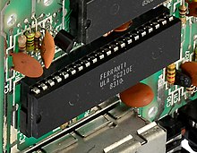
Sinclair Research ported an enhanced ZX80 design to a ULA chip for the ZX81, and later used a ULA in the ZX Spectrum. A compatible chip was made in Russia as T34VG1.[9] Acorn Computers used several ULA chips in the BBC Micro, and later a single ULA for the Acorn Electron. Many other manufacturers from the time of the home computer boom period used ULAs in their machines. The IBM PC took over much of the personal computer market, and the sales volumes made full-custom chips more economical. Commodore's Amiga series used gate arrays for the Gary and Gayle custom-chips, as their code-names may suggest.
Boom[]
While the market boomed, profits for the industry were lacking. Semiconductors underwent a series of rolling recessions during the 1980s that created a boom-bust cycle. The 1980 and 1981-1982 general recessions were followed by high interest rates that curbed capital spending. This reduction played havoc on the semiconductor business that at the time was highly dependent on capital spending. Manufacturers desperate to keep their fab plants full and afford constant modernization in a fast moving industry became hyper-competitive. The many new entrants to the market drove gate array prices down to the marginal costs of the silicon manufacturers. Fabless companies such as LSI Logic and CDI survived on selling design services and computer time rather than on the production revenues.[6]
Indirect competition arose with the development of the field-programmable gate array (FPGA). Xilinx was founded in 1984 and its first products were much like early gate arrays, slow and expensive, fit only for some niche markets. However, Moore's Law quickly made them a force and by the early 1990s were seriously disrupting the gate array market.
Designers still wished for a way to create their own complex chips without the expense of full-custom design, and eventually this wish was granted with the arrival of not only the FPGA, but complex programmable logic device (CPLD), metal configurable standard cells (MCSC), and structured ASICs. Whereas a gate array required a back end semiconductor wafer foundry to deposit and etch the interconnections, the FPGA and CPLD had user programmable interconnections. Today's approach is to make the prototypes by FPGAs, as the risk is low and the functionality can be verified quickly. For smaller devices, production cost are sufficiently low. But for large FPGAs, production is very expensive, power hungry, and in many cases do not reach the required speed. To address these issues, several ASIC companies like BaySand, Faraday, Gigoptics and others offer FPGA to ASIC conversion services.
Decline[]
As of the early 21st century, the gate array market was a remnant of its former self, driven by the FPGA conversions done for cost or performance reasons. IMI moved out of gate arrays into mixed signal circuits and was later acquired by Cypress Semiconductor in 2001; CDI closed its doors in 1989; and LSI Logic abandoned the market in favor of standard products and was eventually acquired by Broadcom.[10]
References[]
- ^ The 224 Cell Uncommitted Array Family. Ferranti Electronic Components Division. March 1977. p. 1. Retrieved 23 February 2021.
- ^ Grierson, J. R. (July 1983). "The Use of Gate Arrays in Telecommunications". British Telecommunications Engineering. 2 (2): 78–80. ISSN 0262-401X. Retrieved 26 February 2021.
In the UK, Ferranti, with their bipolar collector diffused isolation (CDI) arrays, pioneered the commercial use of gate arrays and for many years this was by far the most widely used technology.
- ^ "Everybody's talking about Ferranti ICs". British Telecom Journal. Vol. 3, no. 4. January 1983. Retrieved 23 January 2021.
- ^ Ferranti Discrete and Integrated Circuits Quick Reference Guide. Ferranti plc. 1984. pp. IC4. Retrieved 23 February 2021.
- ^ a b c "1967: Application Specific Integrated Circuits employ Computer-Aided Design". The Silicon Engine. Computer History Museum. Retrieved 2018-01-28.
- ^ a b c "Lipp, Bob oral history". Computer History Museum. Retrieved 2018-01-28.
- ^ "People". The Silicon Engine. Computer History Museum. Retrieved 2018-01-28.
- ^ "LSI Logic oral history panel | 102746194". Computer History Museum. Retrieved 2018-01-28.
- ^ Т34ВГ1 — article about the ZX Spectrum ULA compatible chip (in Russian)
- ^ "Companies". The Silicon Engine. Computer History Museum. Retrieved 2018-01-28.
External links[]
 Media related to Gate arrays at Wikimedia Commons
- Gate arrays