Immersion lithography

Immersion lithography is a photolithography resolution enhancement technique for manufacturing integrated circuits (ICs) that replaces the usual air gap between the final lens and the wafer surface with a liquid medium that has a refractive index greater than one. The resolution is increased by a factor equal to the refractive index of the liquid. Current immersion lithography tools use highly purified water for this liquid, achieving feature sizes below 45 nanometers.[1] ASML and Nikon are currently the only manufacturers of immersion lithography systems.
The idea for immersion lithography was first proposed by Taiwanese engineer Burn J. Lin and realized in the 1980s.[2] The same year, IBM's director of silicon technology, Ghavam Shahidi, announced that IBM plans to commercialize lithography based on light filtered through water.[3] Immersion lithography is now being extended to sub- nodes through the use of multiple patterning.
The ability to resolve features in optical lithography is directly related to the numerical aperture of the imaging equipment, the numerical aperture being the sine of the maximum refraction angle multiplied by the refractive index of the medium through which the light travels. The lenses in the highest resolution "dry" photolithography scanners focus light in a cone whose boundary is nearly parallel to the wafer surface. As it is impossible to increase resolution by further refraction, additional resolution is obtained by inserting an immersion medium with a higher index of refraction between the lens and the wafer. The blurriness is reduced by a factor equal to the refractive index of the medium. For example, for water immersion using ultraviolet light at 193 nm wavelength, the index of refraction is 1.44.
The resolution enhancement from immersion lithography is about 30–40% (depending on materials used). However,[clarification needed] the depth of focus, or tolerance in wafer topography flatness, is improved compared to the corresponding "dry" tool at the same resolution.[4]
Defects[]
Defect concerns, e.g., water left behind (watermarks) and loss of resist-water adhesion (air gap or bubbles), have led to considerations of using a topcoat layer directly on top of the photoresist.[5] This topcoat would serve as a barrier for chemical diffusion between the liquid medium and the photoresist. In addition, the interface between the liquid and the topcoat would be optimized for watermark reduction. At the same time, defects from topcoat use should be avoided.
Topcoats have now been tuned for use as antireflection coatings, especially for hyper-NA (NA>1) cases.[6]
By 2008, defect counts on wafers printed by immersion lithography had reached zero level capability.[7]
Polarization impacts[]
Polarization effects due to high angles of interference in the photoresist also have to be considered as features approach 40 nm.[8] Hence, illumination sources generally will need to be azimuthally polarized to match the pole illumination for ideal line-space imaging.[9]
Throughput[]
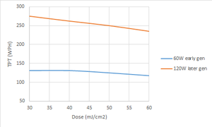
Immersion lithography tools currently boast the highest throughputs (275 WPH) as targeted for high volume manufacturing.[10] This is achieved through higher stage speeds,[11][12] which in turn, are allowed by higher power ArF laser pulse sources.[13] Specifically, the throughput is directly proportional to stage speed V, which is related to dose D and rectangular slit width S and slit intensity Iss (which is directly related to pulse power) by V=Iss*S/D. The slit height is the same as the field height. The slit width S, in turn, is limited by the number of pulses to make the dose (n), divided by the frequency of the laser pulses (f), at the maximum scan speed Vmax by S=Vmax*n/f.[11] At a fixed frequency f and pulse number n, the slit width will be proportional to the maximum stage speed. Hence, throughput at a given dose is improved by increasing maximum stage speed as well as increasing pulse power.
Multiple patterning[]

The resolution limit for a 1.35 NA immersion tool operating at 193 nm wavelength is 36 nm. Going beyond this limit in half-pitch requires multiple patterning. At the 20nm foundry and memory nodes and beyond, double patterning and triple patterning are already being used with immersion lithography for the densest layers.
References[]
- ^ "DailyTech - IDF09 Intel Demonstrates First 22nm Chips Discusses Die Shrink Roadmap". Archived from the original on 2010-08-28. Retrieved 2009-12-07.
- ^ Burn J. Lin (1987). "The future of subhalf-micrometer optical lithography". Microelectronic Engineering 6, 31–51
- ^ "A Whole New World of Chips". Business Week. Archived from the original on 2011-02-21.
- ^ B. J. Lin, J. Microlith Microfab. Microsyst. 1, 7 (2002).
- ^ Y. Wei and R. L. Brainard, Advanced Processes for 193-nm Immersion Lithography, (c) SPIE 2009, Ch.6.
- ^ J. C. Jung et al., Proc. SPIE 5753 (2005).
- ^ B. Rathsack et al., Proc. SPIE 6924, 69244W (2008).
- ^ C. Wagner et al., Proc. SPIE vol. 4000, pp. 344-357 (2000).
- ^ B. W. Smith, L. V. Zavyalova, and A. Estroff, Proc. SPIE 5377 (2004).
- ^ NXT:1980Di
- ^ a b M. A. van den Brink et al., Proc. SPIE 2726, 734 (1996).
- ^ I. Bouchoms et al., Proc. SPIE 8326, 83260L (2012)
- ^ Cymer 120W ArFi source
- Lithography (microfabrication)
- Taiwanese inventions