OR gate
This article needs additional citations for verification. (September 2012) |
| Input | Output | |
| A | B | A OR B |
| 0 | 0 | 0 |
| 0 | 1 | 1 |
| 1 | 0 | 1 |
| 1 | 1 | 1 |
The OR gate is a digital logic gate that implements logical disjunction (∨) from mathematical logic – it behaves according to the truth table above. A HIGH output (1) results if one or both the inputs to the gate are HIGH (1). If neither input is high, a LOW output (0) results. In another sense, the function of OR effectively finds the maximum between two binary digits, just as the complementary AND function finds the minimum.[1]
Symbols[]
There are two symbols of OR gates: the American (ANSI or 'military') symbol and the IEC ('European' or 'rectangular') symbol, as well as the deprecated DIN symbol.[2][3] For more information see Logic Gate Symbols.


Hardware description and pinout[]

OR gates are basic logic gates, and are available in TTL and CMOS ICs logic families. The standard 4000 series CMOS IC is the 4071, which includes four independent two-input OR gates. The TTL device is the 7432. There are many offshoots of the original 7432 OR gate, all having the same pinout but different internal architecture, allowing them to operate in different voltage ranges and/or at higher speeds. In addition to the standard 2-input OR gate, 3- and 4-input OR gates are also available. In the CMOS series, these are:
- 4075: triple 3-input OR gate
- 4072: dual 4-input OR gate
Variations include:
- 74LS32: quad 2-input OR gate (low power Schottky version)
- 74HC32: quad 2-input OR gate (high speed CMOS version) - has lower current consumption/wider voltage range
- 74AC32: quad 2-input OR gate (advanced CMOS version) - similar to 74HC32, but with significantly faster switching speeds and stronger drive
- 74LVC32: low voltage CMOS version of the same.
Implementations[]


Analytical representation[]
is the analytical representation of OR gate:


Alternatives[]
If no specific OR gates are available, one can be made from NAND or NOR gates in the configuration shown in the image below. Any logic gate can be made from a combination of NAND or NOR gates.
| Desired gate | NAND construction | NOR construction |
|---|---|---|
 |
 |

|
Wired-OR[]

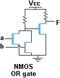
With active low open collector logic outputs, as used for control signals in many circuits, an OR function can be produced by wiring together several outputs. This arrangement is called a wired OR. This implementation of an OR function typically is also found in integrated circuits of N or P-type only transistor processes.
See also[]
| Wikimedia Commons has media related to OR gates. |
References[]
- ^ "OR Gate". Hyperphysics.phy-astr.gsu.edu. Retrieved 2012-09-24.
- ^ Harris, David Harris, Sarah (2007). Digital design and computer architecture (1st ed.). San Francisco,Calif.: Morgan Kaufmann. p. 21. ISBN 9780123704979.
- ^ Brumbach, Michael E. Industrial electricity (8th ed.). Clifton Park, N.Y.: Delmar. p. 546. ISBN 9781435483743.
| hide | ||
|---|---|---|
 | ||
| ||


- Logic gates
- Boolean algebra
- Digital electronics