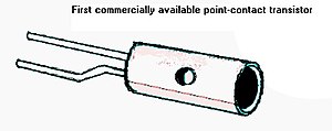
Point-contact transistor
This article needs additional citations for verification. (October 2010) |
The point-contact transistor was the first type of transistor to be successfully demonstrated. It was developed by research scientists John Bardeen and Walter Brattain at Bell Laboratories in December 1947.[1][2] They worked in a group led by physicist William Shockley. The group had been working together on experiments and theories of electric field effects in solid state materials, with the aim of replacing vacuum tubes with a smaller device that consumed less power.
The critical experiment, carried out on December 16, 1947, consisted of a block of germanium, a semiconductor, with two very closely spaced gold contacts held against it by a spring. Brattain attached a small strip of gold foil over the point of a plastic triangle — a configuration which is essentially a point-contact diode. He then carefully sliced through the gold at the tip of the triangle. This produced two electrically isolated gold contacts very close to each other.
The piece of germanium used had a surface layer with an excess of electrons. When an electric signal traveled in through the gold foil, it injected holes (points which lack electrons). This created a thin layer which had a scarcity of electrons.
A small positive current applied to one of the two contacts had an influence on the current which flowed between the other contact and the base upon which the block of germanium was mounted. In fact, a small change in the first contact current caused a greater change in the second contact current; thus it was an amplifier. The first contact is the "emitter" and the second contact is the "collector". The low-current input terminal into the point-contact transistor is the emitter, while the output high current terminals are the base and collector. This differs from the later type of bipolar junction transistor invented in 1951 that operates as transistors still do, with the low current input terminal as the base and the two high current output terminals as the emitter and collector.
The point-contact transistor was commercialized and sold by Western Electric and others but was soon superseded by the bipolar junction transistor, which was easier to manufacture and more rugged.
Forming[]
While point-contact transistors usually worked fine when the metal contacts were simply placed close together on the germanium base crystal, it was desirable to obtain as high an α current gain as possible.
To obtain a higher α current gain in a point-contact transistor, a brief high-current pulse was used to modify the properties of the collector point of contact, a technique called 'electrical forming'. Usually this was done by charging a capacitor of a specified value to a specified voltage then discharging it between the collector and the base electrodes. Forming had a significant failure rate, so many commercial encapsulated transistors had to be discarded. While the effects of forming were understood empirically, the exact physics of the process could never be adequately studied and thus no clear theory was ever developed to explain it or provide guidance on improving it.
Unlike later semiconductor devices, it was possible for an amateur to make a point-contact transistor, starting with a germanium point-contact diode as a source of material (even a burnt-out diode could be used; and the transistor could be re-formed if damaged, several times if necessary).[3]
Characteristics[]
Some characteristics of point-contact transistors differ from the later junction transistor:
- The common base current gain (or α) of a point-contact transistor is around 2 to 3, whereas α of bipolar junction transistor (BJT) cannot exceed 1 and the common emitter current gain (or β) of a point-contact transistor cannot exceed 1, whereas β of a BJT is typically between 20 and 200.
- Differential negative resistance.
- When used in the saturated mode in digital logic, in some circuit designs (but not all) they latched in the on-state, making it necessary to remove power for a short time in each machine cycle to return them to the off-state.
See also[]
- Crystal radio
- Duodiode
- Transistron
References[]
- ^ Hoddeson, Lillian (1981). "The Discovery of the Point-Contact Transistor". Historical Studies in the Physical Sciences. University of California Press. 12 (1): 41–76. doi:10.2307/27757489.
- ^ Cressler, John (2017). Silicon Earth: Introduction to Microelectronics and Nanotechnology (2 ed.). CRC Press. p. 3-22. ISBN 9781351830201.
- ^ HOME-MADE TRANSISTORS: P B Helsdon, Wirless World, January 1954. Article starts "It is quite practicable to make point-contact transistors at home which compare quite well with those advertised by professional manufacturers."
Further reading[]
- Bardeen, J.; Brattain, W.H. (15 July 1948). "The Transistor, A Semiconductor Triode". Physical Review. American Physical Society. 74 (2): 230–231. doi:10.1103/physrev.74.230.
External links[]
- Transistor types
- Bipolar transistors
- Computer-related introductions in 1947