Single-layer materials
In materials science, the term single-layer materials or 2D materials refers to crystalline solids consisting of a single layer of atoms. These materials are promising for some applications but remain the focus of research. Single-layer materials derived from single elements generally carry the -ene suffix in their names, e.g. graphene. Single-layer materials that are compounds of two or more elements have -ane or -ide suffixes. 2D materials can generally be categorized as either 2D allotropes of various elements or as compounds (consisting of two or more covalently bonding elements).
It is predicted that there are hundreds of stable single-layer materials.[1][2]
Single element materials[]
C: graphene and graphyne[]
- Graphene
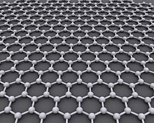
Graphene is a crystalline allotrope of carbon in the form of a nearly transparent (to visible light) one atom thick sheet. It is hundreds of times stronger than most steels by weight.[3] It has the highest known thermal and electrical conductivity, displaying current densities 1,000,000 times that of copper.[4] It was first produced in 2004.[5]
Andre Geim and Konstantin Novoselov won the 2010 Nobel Prize in Physics "for groundbreaking experiments regarding the two-dimensional material graphene". They first produced it by lifting graphene flakes from bulk graphite with adhesive tape and then transferring them onto a silicon wafer.[6]
- Graphyne
Graphyne is another 2-dimensional carbon allotrope whose structure is similar to graphene's. It can be seen as a lattice of benzene rings connected by acetylene bonds. Depending on the content of the acetylene groups, graphyne can be considered a mixed hybridization, spn, where 1 < n < 2,[7][8] and versus graphene's (pure sp2) and diamond (pure sp3).
First-principle calculations using phonon dispersion curves and ab-initio finite temperature, quantum mechanical molecular dynamics simulations showed graphyne and its boron nitride analogues to be stable.[9]
The existence of graphyne was conjectured before 1960.[10] It has not yet been synthesized. However, graphdiyne (graphyne with diacetylene groups) was synthesized on copper substrates.[11] Recently, it has been claimed to be a competitor for graphene due to the potential of direction-dependent Dirac cones.[12][13]
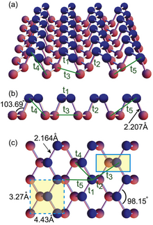
B: borophene[]

36 cluster might be seen as smallest borophene; front and side view
Borophene is a crystalline atomic monolayer of boron and is also known as boron sheet. First predicted by theory in the mid-1990s in a freestanding state,[14] and then demonstrated as distinct monoatomic layers on substrates by Zhang et al.,[15] different borophene structures were experimentally confirmed in 2015.[16][17]
Ge: germanene[]
Germanene is a two-dimensional allotrope of germanium with a buckled honeycomb structure.[18] Experimentally synthesized germanene exhibits a honeycomb structure.[19][20] This honeycomb structure consists of two hexagonal sub-lattices that are vertically displaced by 0.2 A from each other.[21]
Si: silicene[]

Silicene is a two-dimensional allotrope of silicon, with a hexagonal honeycomb structure similar to that of graphene.[22][23][24]
Sn: stanene[]

Stanene is a predicted topological insulator that may display dissipationless currents at its edges near room temperature. It is composed of tin atoms arranged in a single layer, in a manner similar to graphene.[25] Its buckled structure leads to high reactivity against common air pollutions such as NOx and COx and is able to trap and dissociate them at low temperature.[26] Recently structure determination of stanene is done using low energy electron diffraction and it shows very interesting result of ultra-flat stanene on Cu(111) surface.[27]
Pb: plumbene[]
Plumbene is a two-dimensional allotrope of lead, with a hexagonal honeycomb structure similar to that of graphene.[28]
P: phosphorene[]
Phosphorene is a 2-dimensional, crystalline allotrope of phosphorus. Its mono-atomic hexagonal structure makes it conceptually similar to graphene. However, phosphorene has substantially different electronic properties; in particular it possesses a nonzero band gap while displaying high electron mobility.[29] This property potentially makes it a better semiconductor than graphene.[30] The synthesis of phosphorene mainly consists of micromechanical cleavage or liquid phase exfoliation methods. The former has a low yield while the latter produce free standing nanosheets in solvent and not on the solid support. The bottom-up approaches like chemical vapor deposition (CVD) are still blank because of its high reactivity. Therefore, in the current scenario, the most effective method for large area fabrication of thin films of phosphorene consists of wet assembly techniques like Langmuir-Blodgett involving the assembly followed by deposition of nanosheets on solid supports[31]
Sb: antimonene[]
Antimonene is a two-dimensional allotrope of antimony, with its atoms arranged in a buckled honeycomb lattice. Theoretical calculations[32] predicted that antimonene would be a stable semiconductor in ambient conditions with suitable performance for (opto)electronics. Antimonene was first isolated in 2016 by micromechanical exfoliation[33] and it was found to be very stable under ambient conditions. Its properties make it also a good candidate for biomedical and energy applications.[34]
In a study made in 2018,[35] antimonene modified screen-printed electrodes (SPE’s) were subjected to a galvanostatic charge/discharge test using a two-electrode approach to characterize their supercapacitive properties. The best configuration observed, which contained 36 nanograms of antimonene in the SPE, showed a specific capacitance of 1578 F g−1 at a current of 14 A g−1. Over 10,000 of these galvanostatic cycles, the capacitance retention values drop to 65% initially after the first 800 cycles, but then remain between 65% and 63% for the remaining 9,200 cycles. The 36 ng antimonene/SPE system also showed an energy density of 20 mW h kg−1 and a power density of 4.8 kW kg−1. These supercapacitive properties indicate that antimonene is a promising electrode material for supercapacitor systems.
Bi: bismuthene[]
Bismuthene, the two-dimensional allotrope of bismuth, was predicted to be a topological insulator. It was predicted that bismuthene retains its topological phase when grown on silicon carbide in 2015.[36] The prediction was successfully realized and synthesized in 2016.[37] At first glance the system is similar to graphene, as the Bi atoms arrange in a honeycomb lattice. However the bandgap is as large as 800mV due to the large of the Bi atoms and their interaction with the substrate. Thus, room-temperature applications of the quantum spin Hall effect come into reach. Top-down exfoliation of bismuthene has been reported in various instances [38][39] with recent works promoting the implementation of bismuthene in the field of electrochemical sensing.[40][41]
Metals[]

Single and double atom layers of platinum in a two-dimensional film geometry has been demonstrated.[43][44] These atomically thin platinum films are epitaxially grown on graphene[43] which imposes a compressive strain that modifies the surface chemistry of the platinum, while also allowing charge transfer through the graphene.[44] Single atom layer of palladium with the thickness down to 2.6 Å,[42] and rhodium with the thickness of less than 4 Å [45] have also been synthesized and characterized with atomic force microscopy and transmission electron microscopy.
2D alloys[]
Two-dimensional alloys is single atomic layer of alloy that is incommensurate with underlying substrate. One example is the 2D ordered alloys of Pb with Sn and with Bi.[46][47]
2D supracrystals[]
The supracrystals of 2D materials have been proposed and theoretically simulated.[48][49] These monolayer crystals are built of supra atomic periodic structures where atoms in the nodes of the lattice are replaced by symmetric complexes. For example, in the hexagonal structure of graphene patterns of 4 or 6 carbon atoms would be arranged hexagonally instead of single atoms, as the repeating node in the unit cell.
Compounds[]

- Graphane, (CH)
n - Boron nitride nanosheet

- Germanane
Germanane is a single-layer crystal composed of germanium with one hydrogen bonded in the z-direction for each atom.[50] Germanane’s structure is similar to graphane,[51] Bulk germanium does not adopt this structure. Germanane is produced in a two-step route starting with . From this material, the calcium (Ca) is removed by de-intercalation with HCl to give a layered solid with the empirical formula GeH.[52] The Ca sites in Zintyl-phase CaGe
2 interchange with the hydrogen atoms in the HCl solution, producing GeH and CaCl2.
Organic[]
Ni3(HITP)2 is an organic, crystalline, structurally tunable electrical conductor with a high surface area. HITP is an organic chemical (2,3,6,7,10,11-hexaaminotriphenylene). It shares graphene's hexagonal honeycomb structure. Multiple layers naturally form perfectly aligned stacks, with identical 2-nm openings at the centers of the hexagons. Room temperature electrical conductivity is ~40 S cm−1, comparable to that of bulk graphite and among the highest for any conducting metal-organic frameworks (MOFs). The temperature dependence of its conductivity is linear at temperatures between 100 K and 500 K, suggesting an unusual charge transport mechanism that has not been previously observed in organic semiconductors.[53]
The material was claimed to be the first of a group formed by switching metals and/or organic compounds. The material can be isolated as a powder or a film with conductivity values of 2 and 40 S cm−1, respectively.[54]
Combinations[]
Single layers of 2D materials can be combined into layered assemblies.[55] For example, bilayer graphene is a material consisting of two layers of graphene. One of the first reports of bilayer graphene was in the seminal 2004 Science paper by Geim and colleagues, in which they described devices "which contained just one, two, or three atomic layers". Layered combinations of different 2D materials are generally called van der Waals heterostructures. Twistronics is the study of how the angle (the twist) between layers of two-dimensional materials can change their electrical properties.
Characterization[]
Microscopy techniques such as transmission electron microscopy,[56][57][58] 3D electron diffraction,[59] scanning probe microscopy,[60] scanning tunneling microscope,[56] and atomic-force microscopy[56][58][60] are used to characterize the thickness and size of the 2D materials. Electrical properties and structural properties such as composition and defects are characterized by Raman spectroscopy,[56][58][60] X-ray diffraction,[56][58] and X-ray photoelectron spectroscopy.[61]
Applications[]
The major expectation held amongst researchers is that given their exceptional properties, 2D materials will replace conventional semiconductors to deliver a new generation of electronics.
Biological applications[]
Research on 2D nanomaterials is still in its infancy, with the majority of research focusing on elucidating the unique material characteristics and few reports focusing on biomedical applications of 2D nanomaterials.[62] Nevertheless, recent rapid advances in 2D nanomaterials have raised important yet exciting questions about their interactions with biological moieties. 2D nanoparticles such as carbon-based 2D materials, silicate clays, transition metal dichalcogenides (TMDs), and transition metal oxides (TMOs) provide enhanced physical, chemical, and biological functionality owing to their uniform shapes, high surface-to-volume ratios, and surface charge.
Two-dimensional (2D) nanomaterials are ultrathin nanomaterials with a high degree of anisotropy and chemical functionality.[63] 2D nanomaterials are highly diverse in terms of their mechanical, chemical, and optical properties, as well as in size, shape, biocompatibility, and degradability.[64][65] These diverse properties make 2D nanomaterials suitable for a wide range of applications, including drug delivery, imaging, tissue engineering, and biosensors, among others.[66] However, their low-dimension nanostructure gives them some common characteristics. For example, 2D nanomaterials are the thinnest materials known, which means that they also possess the highest specific surface areas of all known materials. This characteristic makes these materials invaluable for applications requiring high levels of surface interactions on a small scale. As a result, 2D nanomaterials are being explored for use in drug delivery systems, where they can adsorb large numbers of drug molecules and enable superior control over release kinetics.[67] Additionally, their exceptional surface area to volume ratios and typically high modulus values make them useful for improving the mechanical properties of biomedical nanocomposites and nanocomposite hydrogels, even at low concentrations. Their extreme thinness has been instrumental for breakthroughs in biosensing and gene sequencing. Moreover, the thinness of these molecules allows them to respond rapidly to external signals such as light, which has led to utility in optical therapies of all kinds, including imaging applications, photothermal therapy (PTT), and photodynamic therapy (PDT).
Despite the rapid pace of development in the field of 2D nanomaterials, these materials must be carefully evaluated for biocompatibility in order to be relevant for biomedical applications.[68] The newness of this class of materials means that even the relatively well-established 2D materials like graphene are poorly understood in terms of their physiological interactions with living tissues. Additionally, the complexities of variable particle size and shape, impurities from manufacturing, and protein and immune interactions have resulted in a patchwork of knowledge on the biocompatibility of these materials.
Related articles[]
References[]
- ^ Ashton, M.; Paul, J.; Sinnott, S. B.; Hennig, R. G. (2017). "Topology-Scaling Identification of Layered Solids and Stable Exfoliated 2D Materials". Phys. Rev. Lett. 118 (10): 106101. arXiv:1610.07673. Bibcode:2017PhRvL.118j6101A. doi:10.1103/PhysRevLett.118.106101. PMID 28339265. S2CID 32012137.
- ^ "MaterialsWeb.org - Databases of Structural, Electronic, and Thermodynamic data for 2D and 3D Materials".
- ^ Andronico, Michael (14 April 2014). "5 Ways Graphene Will Change Gadgets Forever". Laptop.
- ^ "Graphene properties". www.graphene-battery.net. 2014-05-29. Retrieved 2014-05-29.
- ^ "This Month in Physics History: October 22, 2004: Discovery of Graphene". APS News. Series II. 18 (9): 2. 2009.
- ^ "The Nobel Prize in Physics 2010". The Nobel Foundation. Retrieved 2013-12-03.
- ^ Heimann, R.B.; Evsvukov, S.E.; Koga, Y. (1997). "Carbon allotropes: a suggested classification scheme based on valence orbital hybridization". Carbon. 35 (10–11): 1654–1658. doi:10.1016/S0008-6223(97)82794-7.
- ^ Enyashin, Andrey N.; Ivanovskii, Alexander L. (2011). "Graphene Allotropes". Physica Status Solidi B. 248 (8): 1879–1883. Bibcode:2011PSSBR.248.1879E. doi:10.1002/pssb.201046583.
- ^ Özçelik, V. Ongun; Ciraci, S. (January 10, 2013). "Size Dependence in the Stabilities and Electronic Properties of α-Graphyne and Its Boron Nitride Analogue". The Journal of Physical Chemistry C. 117 (5): 2175–2182. arXiv:1301.2593. doi:10.1021/jp3111869. hdl:11693/11999. S2CID 44136901.
- ^ Balaban AT, Rentia CC, Ciupitu E (1968). "Chemical graphs. 6. Estimation of relative stability of several planar and tridimensional lattices for elementary carbon". . 13 (2): 231–.
- ^ Li, Guoxing; Li, Yuliang; Liu, Huibiao; Guo, Yanbing; Li, Yongjun; Zhu, Daoben (2010). "Architecture of graphdiyne nanoscale films". Chemical Communications. 46 (19): 3256–3258. doi:10.1039/B922733D. PMID 20442882. S2CID 43416849.
- ^ Gopalakrishnan, K.; Moses, Kota; Govindaraj, A.; Rao, C. N. R. (2013-12-01). "Supercapacitors based on nitrogen-doped reduced graphene oxide and borocarbonitrides". Solid State Communications. Special Issue: Graphene V: Recent Advances in Studies of Graphene and Graphene analogues. 175–176: 43–50. Bibcode:2013SSCom.175...43G. doi:10.1016/j.ssc.2013.02.005.
- ^ Schirber, Michael (24 February 2012). "Focus: Graphyne May Be Better than Graphene". Physics. 5 (24): 24. Bibcode:2012PhyOJ...5...24S. doi:10.1103/Physics.5.24.
- ^ Boustani, Ihsan (January 1997). "New quasi-planar surfaces of bare boron". Surface Science. 370 (2–3): 355–363. Bibcode:1997SurSc.370..355B. doi:10.1016/S0039-6028(96)00969-7.
- ^ Zhang, Z.; Yang, Y.; Gao, G.; Yakobson, B.I. (2 September 2015). "Two-Dimensional Boron Monolayers Mediated by Metal Substrates". Angewandte Chemie International Edition. 54 (44): 13022–13026. doi:10.1002/anie.201505425. PMID 26331848.
- ^ Mannix, A. J.; Zhou, X.-F.; Kiraly, B.; Wood, J. D.; Alducin, D.; Myers, B. D.; Liu, X.; Fisher, B. L.; Santiago, U.; Guest, J. R.; et al. (17 December 2015). "Synthesis of borophenes: Anisotropic, two-dimensional boron polymorphs". Science. 350 (6267): 1513–1516. Bibcode:2015Sci...350.1513M. doi:10.1126/science.aad1080. PMC 4922135. PMID 26680195.
- ^ Feng, Baojie; Zhang, Jin; Zhong, Qing; Li, Wenbin; Li, Shuai; Li, Hui; Cheng, Peng; Meng, Sheng; Chen, Lan; Wu, Kehui (28 March 2016). "Experimental realization of two-dimensional boron sheets". Nature Chemistry. 8 (6): 563–568. arXiv:1512.05029. Bibcode:2016NatCh...8..563F. doi:10.1038/nchem.2491. PMID 27219700. S2CID 19475989.
- ^ Bampoulis, P.; Zhang, L.; Safaei, A.; van Gastel, R.; Poelsema, B.; Zandvliet, H. J. W. (2014). "Germanene termination of Ge2Pt crystals on Ge(110)". Journal of Physics: Condensed Matter. 26 (44): 442001. arXiv:1706.00697. Bibcode:2014JPCM...26R2001B. doi:10.1088/0953-8984/26/44/442001. PMID 25210978. S2CID 36478002.
- ^ Derivaz, Mickael and Dentel, Didier and Stephan, Regis and Hanf, Marie-Christine and Mehdaoui, Ahmed and Sonnet, Philippe and Pirri, Carmelo (2015). "Continuous germanene layer on Al (111)". Nano Letters. ACS Publications. 15 (4): 2510–2516. Bibcode:2015NanoL..15.2510D. doi:10.1021/acs.nanolett.5b00085. PMID 25802988.CS1 maint: multiple names: authors list (link)
- ^ Yuhara, J.; Shimazu, H.; Ito, K.; Ohta, A.; Kurosawa, M.; Nakatake, M.; Le Lay, Guy (2018). "Germanene Epitaxial Growth by Segregation through Ag(111) Thin Films on Ge(111)". ACS Nano. 12 (11): 11632–11637. doi:10.1021/acsnano.8b07006. PMID 30371060.
- ^ Lee, Kangho; Kim, Hye-Young; Lotya, Mustafa; Coleman, Jonathan N.; Kim, Gyu-Tae; Duesberg, Georg S. (2011-09-22). "Electrical Characteristics of Molybdenum Disulfide Flakes Produced by Liquid Exfoliation". Advanced Materials. 23 (36): 4178–4182. doi:10.1002/adma.201101013. PMID 21823176.
- ^ Xu, Mingsheng and Liang, Tao and Shi, Minmin and Chen, Hongzheng (2013). "Graphene-like two-dimensional materials". Chemical Reviews. ACS Publications}. 113 (5): 3766–3798. doi:10.1021/cr300263a. PMID 23286380.CS1 maint: multiple names: authors list (link)
- ^ S. Cahangirov, M. Topsakal, E. Aktürk, H. Şahin, and S. Ciraci (2009). "Two- and One-Dimensional Honeycomb Structures of Silicon and Germanium". Phys. Rev. Lett. 102 (23): 236804. arXiv:0811.4412. Bibcode:2009PhRvL.102w6804C. doi:10.1103/PhysRevLett.102.236804. PMID 19658958. S2CID 22106457.CS1 maint: multiple names: authors list (link)
- ^ Stephan, Régis and Hanf, Marie-Christine and Sonnet, Philippe (2014). "Spatial analysis of interactions at the silicene/Ag interface: first principles study". Journal of Physics: Condensed Matter. IOP Publishing. 27 (1): 015002. doi:10.1088/0953-8984/27/1/015002. PMID 25407116.CS1 maint: multiple names: authors list (link)
- ^ Yuhara, J.; Fujii, Y.; Isobe, N.; Nakatake, M.; Lede, X.; Rubio, A.; Le Lay, G. (2018). "Large Area Planar Stanene Epitaxially Grown on Ag(111)". 2D Materials. 5 (2): 025002. Bibcode:2018TDM.....5b5002Y. doi:10.1088/2053-1583/aa9ea0.
- ^ Takahashi, L.; Takahashi, K. (2015). "Low temperature pollutant trapping and dissociation over two-dimensional tin". Physical Chemistry Chemical Physics. 17 (33): 21394–21396. Bibcode:2015PCCP...1721394T. doi:10.1039/C5CP03382A. PMID 26226204. Supporting Information
- ^ Ahmed, Rezwan; Nakagawa, Takeshi; Mizuno, Seigi (2020). "Structure determination of ultra-flat stanene on Cu(111) using low energy electron diffraction". Surface Science. 691: 121498. Bibcode:2020SurSc.69121498A. doi:10.1016/j.susc.2019.121498.
- ^ Yuhara, J.; He, B.; Le Lay, G. (2019). "Graphene's Latest Cousin: Plumbene Epitaxial Growth on a "Nano WaterCube"". Advanced Materials. 31 (27): 1901017. doi:10.1002/adma.201901017. PMID 31074927..
- ^ Berger, Andy (July 17, 2015). "Beyond Graphene, a Zoo of New 2-D Materials". Discover Magazine. Retrieved 2015-09-19.
- ^ Li, L.; Yu, Y.; Ye, G. J.; Ge, Q.; Ou, X.; Wu, H.; Feng, D.; Chen, X. H.; Zhang, Y. (2014). "Black phosphorus field-effect transistors". Nature Nanotechnology. 9 (5): 372–377. arXiv:1401.4117. Bibcode:2014NatNa...9..372L. doi:10.1038/nnano.2014.35. PMID 24584274. S2CID 17218693.
- ^ Ritu, Harneet (2016). "Large Area Fabrication of Semiconducting Phosphorene by Langmuir-Blodgett Assembly". Sci. Rep. 6: 34095. arXiv:1605.00875. Bibcode:2016NatSR...634095K. doi:10.1038/srep34095. PMC 5037434. PMID 27671093.
- ^ Zhang, S.; Yan, Z.; Li, Y.; Chen, Z.; Zeng, H. (2015). "Atomically Thin Arsenene and Antimonene: Semimetal-Semiconductor and Indirect-Direct Band-Gap Transitions". Angew. Chem. Int. Ed. 54 (10): 3112–3115. doi:10.1002/anie.201411246. PMID 25564773.
- ^ Ares, P.; Aguilar-Galindo, F.; Rodríguez-San-Miguel, D.; Aldave, D. A.; Díaz-Tendero, S.; Alcamí, M.; Martín, F.; Gómez-Herrero, J.; Zamora, F. (2016). "Mechanical Isolation of Highly Stable Antimonene under Ambient Conditions". Adv. Mater. 28 (30): 6332–6336. arXiv:1608.06859. Bibcode:2016arXiv160806859A. doi:10.1002/adma.201602128. hdl:10486/672484. PMID 27272099. S2CID 8296292.
- ^ Ares, P.; Palacios, J. J.; Abellán, G.; Gómez-Herrero, J.; Zamora, F. (2018). "Recent progress on antimonene: a new bidimensional material". Adv. Mater. 30 (2): 1703771. doi:10.1002/adma.201703771. hdl:10486/688820. PMID 29076558.
- ^ Martínez‐Periñán, Emiliano; Down, Michael P.; Gibaja, Carlos; Lorenzo, Encarnación; Zamora, Félix; Banks, Craig E. (2018). "Antimonene: A Novel 2D Nanomaterial for Supercapacitor Applications" (PDF). Advanced Energy Materials. 8 (11): 1702606. doi:10.1002/aenm.201702606. hdl:10486/688798. ISSN 1614-6840.
- ^ Hsu, Chia-Hsiu; Huang, Zhi-Quan; Chuang, Feng-Chuan; Kuo, Chien-Cheng; Liu, Yu-Tzu; Lin, Hsin; Bansil, Arun (2015-02-10). "The nontrivial electronic structure of Bi/Sb honeycombs on SiC(0001)". New Journal of Physics. 17 (2): 025005. Bibcode:2015NJPh...17b5005H. doi:10.1088/1367-2630/17/2/025005.
- ^ Reis, Felix; Li, Gang; Dudy, Lenart; Bauernfiend, Maximilian; Glass, Stefan; Hanke, Werner; Thomale, Ronny; Schaefer, Joerg; Claessen, Ralph (July 21, 2017). "Bismuthene on a SiC substrate: A candidate for a high-temperature quantum spin Hall material". Science. 357 (6348): 287–290. arXiv:1608.00812. Bibcode:2017Sci...357..287R. doi:10.1126/science.aai8142. PMID 28663438. S2CID 23323210.
- ^ Qi-Qi, Yang (2 October 2018). "2D bismuthene fabricated via acid-intercalated exfoliation showing strong nonlinear near-infrared responses for mode-locking lasers". Nanoscale. 10 (45): 21106–21115. doi:10.1039/c8nr06797j. PMID 30325397.
- ^ Gusmao, Rui; Sofer, Zdenek; Bousa, Daniel; Pumera, Martin (29 July 2017). "Pnictogens (As, Sb, Bi) Nanosheets by Shear Exfoliation Using Kitchen Blenders for Electrochemical Applications". Angewandte Chemie International Edition. 56 (46): 14417–14422. doi:10.1002/anie.201706389. PMID 28755460.
- ^ Martinez, Carmen C.; Gusmao, Rui; Sofer, Zdenek; Pumera, Martin (2019). "Pnictogen-Based Enzymatic Phenol Biosensors: Phosphorene, Arsenene, Antimonene, and Bismuthene". Angewandte Chemie International Edition. 58 (1): 134–138. doi:10.1002/anie.201808846. PMID 30421531.
- ^ Lazanas, Alexandros Ch.; Tsirka, Kyriaki; Paipetis, Alkiviadis S.; Prodromidis, Mamas I. (2020). "2D bismuthene/graphene modified electrodes for the ultra-sensitive stripping voltammetric determination of lead and cadmium". Electrochimica Acta. 336: 135726. doi:10.1016/j.electacta.2020.135726.
- ^ Jump up to: a b Yin, Xi; Liu, Xinhong; Pan, Yung-Tin; Walsh, Kathleen A.; Yang, Hong (November 4, 2014). "Hanoi Tower-like Multilayered Ultrathin Palladium Nanosheets". Nano Letters. 14 (12): 7188–7194. Bibcode:2014NanoL..14.7188Y. doi:10.1021/nl503879a. PMID 25369350.
- ^ Jump up to: a b Abdelhafiz, Ali; Vitale, Adam; Buntin, Parker; deGlee, Ben; Joiner, Corey; Robertson, Alex; Vogel, Eric M.; Warner, Jamie; Alamgir, Faisal M. (2018). "Epitaxial and atomically thin graphene–metal hybrid catalyst films: the dual role of graphene as the support and the chemically-transparent protective cap". Energy & Environmental Science. 11 (6): 1610–1616. doi:10.1039/c8ee00539g.
- ^ Jump up to: a b Abdelhafiz, Ali; Vitale, Adam; Joiner, Corey; Vogel, Eric; Alamgir, Faisal M. (2015-03-16). "Layer-by-Layer Evolution of Structure, Strain, and Activity for the Oxygen Evolution Reaction in Graphene-Templated Pt Monolayers". ACS Applied Materials & Interfaces. 7 (11): 6180–6188. doi:10.1021/acsami.5b00182. PMID 25730297.
- ^ Duan, Haohong; Yan, Ning; Yu, Rong; Chang, Chun-Ran; Zhou, Gang; Hu, Han-Shi; Rong, Hongpan; Niu, Zhiqiang; Mao, Junjie; Asakura, Hiroyuki; Tanaka, Tsunehiro; Dyson, Paul Joseph; Li, Jun; Li, Yadong (17 January 2014). "Ultrathin rhodium nanosheets". Nature Communications. 5: 3093. Bibcode:2014NatCo...5.3093D. doi:10.1038/ncomms4093. PMID 24435210.
- ^ Yuhara, J.; Schmid, M.; Varga, P. (2003). "A two-dimensional alloy of immiscible metals, The single and binary monolayer films of Pb and Sn on Rh(111)". Phys. Rev. B. 67 (19): 195407. Bibcode:2003PhRvB..67s5407Y. doi:10.1103/PhysRevB.67.195407.
- ^ Yuhara, J.; Yokoyama, M.; Matsui, T. (2011). "Two-dimensional solid solution alloy of Bi-Pb binary films on Rh(111)". J. Appl. Phys. 110 (7): 074314–074314–4. Bibcode:2011JAP...110g4314Y. doi:10.1063/1.3650883.
- ^ Kochaev, A. I.; Karenin, A.A.; Meftakhutdinov, R.M.; Brazhe, R.A. (2012). "2D supracrystals as a promising materials for planar nanoacoustoelectronics". Journal of Physics: Conference Series. 345 (1): 012007. Bibcode:2012JPhCS.345a2007K. doi:10.1088/1742-6596/345/1/012007.
- ^ Brazhe, R. A.; Kochaev, A. I. (2012). "Flexural waves in graphene and 2D supracrystals". Physics of the Solid State. 54 (8): 1612–1614. Bibcode:2012PhSS...54.1612B. doi:10.1134/S1063783412080069. S2CID 120094142.
- ^ Bianco, E.; Butler, S.; Jiang, S.; Restrepo, O. D.; Windl, W.; Goldberger, J. E. (2013). "Stability and Exfoliation of Germanane: A Germanium Graphane Analogue". ACS Nano. 7 (5): 4414–21. doi:10.1021/nn4009406. hdl:1811/54792. PMID 23506286.
- ^ Garcia, J. C.; de Lima, D. B.; Assali, L. V. C.; Justo, J. F. (2011). "Group IV graphene- and graphane-like nanosheets". J. Phys. Chem. C. 115 (27): 13242–13246. arXiv:1204.2875. doi:10.1021/jp203657w. S2CID 98682200.
- ^ "'Germanane' may replace silicon for lighter, faster electronics". KurzweilAI. Retrieved 2013-04-12.
- ^ Sheberla, Dennis; Sun, Lei; Blood-Forsythe, Martin A.; Er, Süleyman; Wade, Casey R.; Brozek, Carl K.; Aspuru-Guzik, Alán; Dincă, Mircea (2014). "High Electrical Conductivity in Ni3(2,3,6,7,10,11-hexaiminotriphenylene)2, a Semiconducting Metal–Organic Graphene Analogue". Journal of the American Chemical Society. 136 (25): 8859–8862. doi:10.1021/ja502765n. PMID 24750124.
- ^ "A new self-assembling graphene-like material for flat semiconductors". KurzweilAI. 2014-05-01. Retrieved 2014-08-24.
- ^ Ipaves, B.; Justo, J.F.; Assali, L. V. C. (2019). "Carbon-Related Bilayers: Nanoscale Building Blocks for Self-Assembly Nanomanufacturing". J. Phys. Chem. C. 123 (37): 23195-23204. arXiv:1908.06218. doi:10.1021/acs.jpcc.9b05446. S2CID 201070776.
- ^ Jump up to: a b c d e Butler, Sheneve Z.; Hollen, Shawna M.; Cao, Linyou; Cui, Yi; Gupta, Jay A.; Gutiérrez, Humberto R.; Heinz, Tony F.; Hong, Seung Sae; Huang, Jiaxing (2013). "Progress, Challenges, and Opportunities in Two-Dimensional Materials Beyond Graphene". ACS Nano. 7 (4): 2898–2926. doi:10.1021/nn400280c. PMID 23464873.
- ^ Bhimanapati, Ganesh R.; Lin, Zhong; Meunier, Vincent; Jung, Yeonwoong; Cha, Judy; Das, Saptarshi; Xiao, Di; Son, Youngwoo; Strano, Michael S. (2015). "Recent Advances in Two-Dimensional Materials beyond Graphene". ACS Nano. 9 (12): 11509–11539. doi:10.1021/acsnano.5b05556. PMID 26544756.
- ^ Jump up to: a b c d Rao, C. N. R.; Nag, Angshuman (2010-09-01). "Inorganic Analogues of Graphene". European Journal of Inorganic Chemistry. 2010 (27): 4244–4250. doi:10.1002/ejic.201000408.
- ^ Sung, S.H.; Schnitzer, N.; Brown, L.; Park, J.; Hovden, R. (2019-06-25). "Stacking, strain, and twist in 2D materials quantified by 3D electron diffraction". Physical Review Materials. 3 (6): 064003. arXiv:1905.11354. Bibcode:2019PhRvM...3f4003S. doi:10.1103/PhysRevMaterials.3.064003. S2CID 166228311.
- ^ Jump up to: a b c Rao, C. N. R.; Ramakrishna Matte, H. S. S.; Maitra, Urmimala (2013-12-09). "Graphene Analogues of Inorganic Layered Materials". Angewandte Chemie International Edition. 52 (50): 13162–13185. doi:10.1002/anie.201301548. PMID 24127325.
- ^ Rao, C. N. R; Maitra, Urmimala (2015-01-01). "Inorganic Graphene Analogs". Annual Review of Materials Research. 45 (1): 29–62. Bibcode:2015AnRMS..45...29R. doi:10.1146/annurev-matsci-070214-021141.
- ^ Kerativitayanan, P; Carrow, JK; Gaharwar, AK (26 May 2015). "Nanomaterials for Engineering Stem Cell Responses". Advanced Healthcare Materials. 4 (11): 1600–27. doi:10.1002/adhm.201500272. PMID 26010739.
- ^ Huang, X; Tan, C; Yin, Z; Zhang, H (9 April 2014). "25th anniversary article: hybrid nanostructures based on two-dimensional nanomaterials". Advanced Materials & Processes. 26 (14): 2185–204. doi:10.1002/adma.201304964. PMID 24615947.
- ^ Carrow, James K.; Gaharwar, Akhilesh K. (February 2015). "Bioinspired Polymeric Nanocomposites for Regenerative Medicine". Macromolecular Chemistry and Physics. 216 (3): 248–264. doi:10.1002/macp.201400427.
- ^ Nandwana, Dinkar; Ertekin, Elif (21 June 2015). "Lattice mismatch induced ripples and wrinkles in planar graphene/boron nitride superlattices". Journal of Applied Physics. 117 (234304): 234304. arXiv:1504.02929. Bibcode:2015JAP...117w4304N. doi:10.1063/1.4922504. S2CID 119251606.
- ^ Gaharwar, AK; Peppas, NA; Khademhosseini, A (March 2014). "Nanocomposite hydrogels for biomedical applications". Biotechnology and Bioengineering. 111 (3): 441–53. doi:10.1002/bit.25160. PMC 3924876. PMID 24264728.
- ^ Goenka, S; Sant, V; Sant, S (10 January 2014). "Graphene-based nanomaterials for drug delivery and tissue engineering". Journal of Controlled Release. 173: 75–88. doi:10.1016/j.jconrel.2013.10.017. PMID 24161530.
- ^ Gaharwar, A.K.; et al. (2013). Nanomaterials in tissue engineering : fabrication and applications. Oxford: Woodhead Publishing. ISBN 978-0-85709-596-1.
Additional reading[]
- Garcia, J. C.; de Lima, D. B.; Assali, L. V. C.; Justo, J. F. (2011). "Group IV graphene- and graphane-like nanosheets". J. Phys. Chem. C. 115 (27): 13242–13246. arXiv:1204.2875. doi:10.1021/jp203657w. S2CID 98682200.
- Xu, Yang; Cheng, Cheng; Du, Sichao; Yang, Jianyi; Yu, Bin; Luo, Jack; Yin, Wenyan; Li, Erping; Dong, Shurong; Ye, Peide; Duan, Xiangfeng (2016). "Contacts between Two- and Three-Dimensional Materials: Ohmic, Schottky, and p–n Heterojunctions". ACS Nano. 10 (5): 4895–4919. doi:10.1021/acsnano.6b01842. PMID 27132492.
- Briggs, Natalie; Subramanian, Shruti; Lin, Zhong; Li, Xufan; Zhang, Xiaotian; Zhang, Kehao; Xiao, Kai; Geohegan, David; Wallace, Robert; Chen, Long-Qing; Terrones, Mauricio; Ebrahimi, Aida; Das, Saptarshi; Redwing, Joan; Hinkle, Christopher; Momeni, Kasra; van Duin, Adri; Crespi, Vin; Kar, Swastik; Robinson, Joshua A. (2019). "A roadmap for electronic grade 2D materials". 2D Materials. 6 (2): 022001. Bibcode:2019TDM.....6b2001B. doi:10.1088/2053-1583/aaf836. OSTI 1503991.
- Shahzad, F.; Alhabeb, M.; Hatter, C. B.; Anasori, B.; Man Hong, S.; Koo, C. M.; Gogotsi, Y. (2016). "Electromagnetic interference shielding with 2D transition metal carbides (MXenes)". Science. 353 (6304): 1137–1140. Bibcode:2016Sci...353.1137S. doi:10.1126/science.aag2421. PMID 27609888.
- "Graphene Uses & Applications". Graphenea. Retrieved 2014-04-13.
- cao, yameng; Robson, Alexander J.; Alharbi, Abdullah; Roberts, Jonathan; Woodhead, Christopher Stephen; Noori, Yasir Jamal; Gavito, Ramon Bernardo; Shahrjerdi, Davood; Roedig, Utz (2017). "Optical identification using imperfections in 2D materials". 2D Materials. 4 (4): 045021. arXiv:1706.07949. Bibcode:2017TDM.....4d5021C. doi:10.1088/2053-1583/aa8b4d. S2CID 35147364.
- Kolesnichenko, Pavel; Zhang, Qianhui; Zheng, Changxi; Fuhrer, Michael; Davis, Jeffrey (2021). "Multidimensional analysis of excitonic spectra of monolayers of tungsten disulphide: toward computer-aided identification of structural and environmental perturbations of 2D materials". Machine Learning: Science and Technology. 2 (2): 025021. doi:10.1088/2632-2153/abd87c.
- Two-dimensional nanomaterials
- Condensed matter physics
- Semiconductors
- Monolayers