Wired logic connection

A wired logic connection is a logic gate that implements boolean algebra (logic) using only active and passive components such as diodes and resistors. A wired logic connection can create an AND or an OR gate. The limitations are the inability to create a NOT gate and the lack of level restoration.
The wired AND connection[]

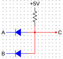
The wired AND connection is a form of AND gate. It uses a pull up resistor and one diode per input to create this function.
The positive voltage from the source is directed away from the output C and towards A and B via the diodes connected directed towards the inputs. When positive logic that is equal to or greater than that of the source is applied to all inputs, the source voltage is directed to the output. The AND gate is capable of an arbitrary number of inputs.
The output C is determined by the inputs at A and B according to the truth table.[1]
| INPUT | OUTPUT | |
|---|---|---|
| A | B | A AND B |
| 0 | 0 | 0 |
| 0 | 1 | 0 |
| 1 | 0 | 0 |
| 1 | 1 | 1 |
The wired AND function is also achieved by using open collector TTL gate outputs instead of diodes. The wired AND function can be achieved by simply tying gate outputs together to a common-collector pull-up resistor.
The wired OR connection[]

The wired OR connection electrically performs the Boolean logic operation of an OR gate, using a pull down resistor and one diode per input.[dubious ]
Voltage from any input is directed through its corresponding diode directly to the output C. If no voltage/logic exists on any input there will be no output. The positive voltage source that is present in the AND connection is replaced by a ground in the OR connection. Also, notice the positioning of the diodes as compared to the AND gate. Similarly, the OR connection is capable of an arbitrary number of inputs and only one output.
The output C is determined by the inputs at A and B according to the truth table and square wave (right).
| INPUT | OUTPUT | |
|---|---|---|
| A | B | A OR B |
| 0 | 0 | 0 |
| 0 | 1 | 1 |
| 1 | 0 | 1 |
| 1 | 1 | 1 |
Reversed levels[]
A wired AND can be converted into a wired OR, and vice versa, by using signals with reversed levels.
For example,
Compatibility of wired AND OR using diodes[]
With the wired AND or OR using diodes it should be cautioned that the output voltage will be shifted positive or negative by a diode drop so that it is likely not compatible with the primary logic family.
References[]
- ^ M. Morris Mano, Digital Logic and Computer Design, Prentice-Hall, 1979 ISBN 0-13-214510-3, page 571
- Digital Techniques, Heathkit Educational Systems,1990
- Fundamental Physics, K.L Gomber and K.L Gogia,Pradeep Publications, 2005
External links[]
- Logic gates


