Hall effect
This article needs additional citations for verification. (January 2018) |
| Articles about |
| Electromagnetism |
|---|
 |

In the diagram A the flat conductor possesses a negative charge on the top (symbolized by the blue color) and a positive charge on the bottom (red color). In sketches B and C the direction of the electrical and the magnetic fields are changed respectively which switches the polarity of the charges around. In the diagram D both fields change direction simultaneously which results in the same polarity as in sketch A.
1 electrons
2 flat conductor, which serves as a hall element (hall effect sensor)
3 magnet
4 magnetic field
5 power source
The Hall effect is the production of a voltage difference (the Hall voltage) across an electrical conductor that is transverse to an electric current in the conductor and to an applied magnetic field perpendicular to the current. It was discovered by Edwin Hall in 1879.[1][2]
A Hall effect can also occur across a void or hole in a semiconductor or metal plate, when current is injected via contacts that lie on the boundary or edge of the void or hole, and the charge flows outside the void or hole, in the metal or semiconductor. This Hall effect becomes observable in a perpendicular applied magnetic field across voltage contacts that lie on the boundary of the void on either side of a line connecting the current contacts, it exhibits apparent sign reversal in comparison to the standard ordinary Hall effect in the simply connected specimen, and this Hall effect depends only on the current injected from within the void.[3]
Superposition may also be realized in the Hall effect: Imagine the standard Hall configuration, a simply connected (void-less) thin rectangular homogeneous Hall plate with current and voltage contacts on the (external) boundary which develops a Hall voltage in a perpendicular magnetic field. Now, imagine placing a rectangular void or hole within this standard Hall configuration, with current and voltage contacts, as mentioned above, on the interior boundary or edge of the void. For simplicity, the current contacts on the boundary of the void may be lined up with the current contacts on the exterior boundary in the standard Hall configuration. In such a configuration, two Hall effects may be realized and observed simultaneously in the same doubly connected device: A Hall effect on the external boundary that is proportional to the current injected only via the outer boundary, and an apparently sign reversed Hall effect on the interior boundary that is proportional to the current injected only via the interior boundary. Multiple Hall effects superposition may be realized by placing multiple voids within the Hall element, with current and voltage contacts on the boundary of each void.[3] DE Patent 4308375
The Hall coefficient is defined as the ratio of the induced electric field to the product of the current density and the applied magnetic field. It is a characteristic of the material from which the conductor is made, since its value depends on the type, number, and properties of the charge carriers that constitutes the current.
For clarity, the original effect is sometimes called the ordinary Hall effect to distinguish it from other "Hall effects", which may have additional physical mechanisms, but built on these basics.
Discovery[]
This section needs expansion. You can help by . (March 2019) |
The modern theory of electromagnetism was systematized by James Clerk Maxwell in the paper "On Physical Lines of Force", which was published in four parts between 1861 and 1862. While Maxwell's paper established a solid mathematical basis for electromagnetic theory, the detailed mechanisms of the theory were still being explored. One such question was about the details of the interaction between magnets and electric current, including whether magnetic fields interacted with the conductors or the electric current itself. In 1879 Edwin Hall was exploring this interaction, and discovered the Hall effect while he was working on his doctoral degree at Johns Hopkins University in Baltimore, Maryland.[4] Eighteen years before the electron was discovered, his measurements of the tiny effect produced in the apparatus he used were an experimental tour de force, published under the name "On a New Action of the Magnet on Electric Currents".[5][6][7]
Theory[]
The Hall effect is due to the nature of the current in a conductor. Current consists of the movement of many small charge carriers, typically electrons, holes, ions (see Electromigration) or all three. When a magnetic field is present, these charges experience a force, called the Lorentz force.[8] When such a magnetic field is absent, the charges follow approximately straight, 'line of sight' paths between collisions with impurities, phonons, etc. However, when a magnetic field with a perpendicular component is applied, their paths between collisions are curved, thus moving charges accumulate on one face of the material. This leaves equal and opposite charges exposed on the other face, where there is a scarcity of mobile charges. The result is an asymmetric distribution of charge density across the Hall element, arising from a force that is perpendicular to both the 'line of sight' path and the applied magnetic field. The separation of charge establishes an electric field that opposes the migration of further charge, so a steady electric potential is established for as long as the charge is flowing.[9]
In classical electromagnetism electrons move in the opposite direction of the current I (by convention "current" describes a theoretical "hole flow"). In some metals and semiconductors it appears "holes" are actually flowing because the direction of the voltage is opposite to the derivation below.

For a simple metal where there is only one type of charge carrier (electrons), the Hall voltage VH can be derived by using the Lorentz force and seeing that, in the steady-state condition, charges are not moving in the y-axis direction. Thus, the magnetic force on each electron in the y-axis direction is cancelled by a y-axis electrical force due to the buildup of charges. The vx term is the drift velocity of the current which is assumed at this point to be holes by convention. The vxBz term is negative in the y-axis direction by the right hand rule.

In steady state, F = 0, so 0 = Ey − vxBz, where Ey is assigned in the direction of the y-axis, (and not with the arrow of the induced electric field ξy as in the image (pointing in the −y direction), which tells you where the field caused by the electrons is pointing).
In wires, electrons instead of holes are flowing, so vx → −vx and q → −q. Also Ey = −VH/w. Substituting these changes gives

The conventional "hole" current is in the negative direction of the electron current and the negative of the electrical charge which gives Ix = ntw(−vx)(−e) where n is charge carrier density, tw is the cross-sectional area, and −e is the charge of each electron. Solving for and plugging into the above gives the Hall voltage:


If the charge build up had been positive (as it appears in some metals and semiconductors), then the VH assigned in the image would have been negative (positive charge would have built up on the left side).
The Hall coefficient is defined as
- or


where j is the current density of the carrier electrons, and Ey is the induced electric field. In SI units, this becomes

(The units of RH are usually expressed as m3/C, or Ω·cm/G, or other variants.) As a result, the Hall effect is very useful as a means to measure either the carrier density or the magnetic field.
One very important feature of the Hall effect is that it differentiates between positive charges moving in one direction and negative charges moving in the opposite. In the diagram above, the Hall effect with a negative charge carrier (the electron) is presented. But consider the same magnetic field and current are applied but the current is carried inside the Hall effect device by a positive particle. The particle would of course have to be moving in the opposite direction of the electron in order for the current to be the same—down in the diagram, not up like the electron is. And thus, mnemonically speaking, your thumb in the Lorentz force law, representing (conventional) current, would be pointing the same direction as before, because current is the same—an electron moving up is the same current as a positive charge moving down. And with the fingers (magnetic field) also being the same, interestingly the charge carrier gets deflected to the left in the diagram regardless of whether it's positive or negative. But if positive carriers are deflected to the left, they would build a relatively positive voltage on the left whereas if negative carriers (namely electrons) are, they build up a negative voltage on the left as shown in the diagram. Thus for the same current and magnetic field, the polarity of the Hall voltage is dependent on the internal nature of the conductor and is useful to elucidate its inner workings.
This property of the Hall effect offered the first real proof that electric currents in most metals are carried by moving electrons, not by protons. It also showed that in some substances (especially p-type semiconductors), it is contrarily more appropriate to think of the current as positive "holes" moving rather than negative electrons. A common source of confusion with the Hall effect in such materials is that holes moving one way are really electrons moving the opposite way, so one expects the Hall voltage polarity to be the same as if electrons were the charge carriers as in most metals and n-type semiconductors. Yet we observe the opposite polarity of Hall voltage, indicating positive charge carriers. However, of course there are no actual positrons or other positive elementary particles carrying the charge in p-type semiconductors, hence the name "holes". In the same way as the oversimplistic picture of light in glass as photons being absorbed and re-emitted to explain refraction breaks down upon closer scrutiny, this apparent contradiction too can only be resolved by the modern quantum mechanical theory of quasiparticles wherein the collective quantized motion of multiple particles can, in a real physical sense, be considered to be a particle in its own right (albeit not an elementary one).[10]
Unrelatedly, inhomogeneity in the conductive sample can result in a spurious sign of the Hall effect, even in ideal van der Pauw configuration of electrodes. For example, a Hall effect consistent with positive carriers was observed in evidently n-type semiconductors.[11] Another source of artifact, in uniform materials, occurs when the sample's aspect ratio is not long enough: the full Hall voltage only develops far away from the current-introducing contacts, since at the contacts the transverse voltage is shorted out to zero.
Hall effect in semiconductors[]
When a current-carrying semiconductor is kept in a magnetic field, the charge carriers of the semiconductor experience a force in a direction perpendicular to both the magnetic field and the current. At equilibrium, a voltage appears at the semiconductor edges.
The simple formula for the Hall coefficient given above is usually a good explanation when conduction is dominated by a single charge carrier. However, in semiconductors and many metals the theory is more complex, because in these materials conduction can involve significant, simultaneous contributions from both electrons and holes, which may be present in different concentrations and have different mobilities. For moderate magnetic fields the Hall coefficient is[12][13]

or equivalently

with

Here n is the electron concentration, p the hole concentration, μe the electron mobility, μh the hole mobility and e the elementary charge.
For large applied fields the simpler expression analogous to that for a single carrier type holds.
Relationship with star formation[]
Although it is well known that magnetic fields play an important role in star formation, research models[14][15][16] indicate that Hall diffusion critically influences the dynamics of gravitational collapse that forms protostars.
Quantum Hall effect[]
For a two-dimensional electron system which can be produced in a MOSFET, in the presence of large magnetic field strength and low temperature, one can observe the quantum Hall effect, in which the Hall conductance σ undergoes quantum Hall transitions to take on the quantized values.
Spin Hall effect[]
The spin Hall effect consists in the spin accumulation on the lateral boundaries of a current-carrying sample. No magnetic field is needed. It was predicted by Mikhail Dyakonov and in 1971 and observed experimentally more than 30 years later, both in semiconductors and in metals, at cryogenic as well as at room temperatures.
Quantum spin Hall effect[]
For mercury telluride two dimensional quantum wells with strong spin-orbit coupling, in zero magnetic field, at low temperature, the quantum spin Hall effect has been recently observed.
Anomalous Hall effect[]
In ferromagnetic materials (and paramagnetic materials in a magnetic field), the Hall resistivity includes an additional contribution, known as the anomalous Hall effect (or the extraordinary Hall effect), which depends directly on the magnetization of the material, and is often much larger than the ordinary Hall effect. (Note that this effect is not due to the contribution of the magnetization to the total magnetic field.) For example, in nickel, the anomalous Hall coefficient is about 100 times larger than the ordinary Hall coefficient near the Curie temperature, but the two are similar at very low temperatures.[17] Although a well-recognized phenomenon, there is still debate about its origins in the various materials. The anomalous Hall effect can be either an extrinsic (disorder-related) effect due to spin-dependent scattering of the charge carriers, or an intrinsic effect which can be described in terms of the Berry phase effect in the crystal momentum space (k-space).[18]
Hall effect in ionized gases[]
The Hall effect in an ionized gas (plasma) is significantly different from the Hall effect in solids (where the Hall parameter is always much less than unity). In a plasma, the Hall parameter can take any value. The Hall parameter, β, in a plasma is the ratio between the electron gyrofrequency, Ωe, and the electron-heavy particle collision frequency, ν:

where
- e is the elementary charge (approximately 1.6×10⁻¹⁹ C)
- B is the magnetic field (in teslas)
- me is the electron mass (approximately 9.1×10⁻³¹ kg).
The Hall parameter value increases with the magnetic field strength.
Physically, the trajectories of electrons are curved by the Lorentz force. Nevertheless, when the Hall parameter is low, their motion between two encounters with heavy particles (neutral or ion) is almost linear. But if the Hall parameter is high, the electron movements are highly curved. The current density vector, J, is no longer collinear with the electric field vector, E. The two vectors J and E make the Hall angle, θ, which also gives the Hall parameter:

Applications[]
Hall probes are often used as magnetometers, i.e. to measure magnetic fields, or inspect materials (such as tubing or pipelines) using the principles of magnetic flux leakage.
Hall effect devices produce a very low signal level and thus require amplification. While suitable for laboratory instruments, the vacuum tube amplifiers available in the first half of the 20th century were too expensive, power consuming, and unreliable for everyday applications. It was only with the development of the low cost integrated circuit that the Hall effect sensor became suitable for mass application. Many devices now sold as Hall effect sensors in fact contain both the sensor as described above plus a high gain integrated circuit (IC) amplifier in a single package. Recent advances have further added into one package an analog-to-digital converter and I²C (Inter-integrated circuit communication protocol) IC for direct connection to a microcontroller's I/O port.
Advantages over other methods[]
Hall effect devices (when appropriately packaged) are immune to dust, dirt, mud, and water. These characteristics make Hall effect devices better for position sensing than alternative means such as optical and electromechanical sensing.

When electrons flow through a conductor, a magnetic field is produced. Thus, it is possible to create a non-contacting current sensor. The device has three terminals. A sensor voltage is applied across two terminals and the third provides a voltage proportional to the current being sensed. This has several advantages; no additional resistance (a shunt, required for the most common current sensing method) need to be inserted in the primary circuit. Also, the voltage present on the line to be sensed is not transmitted to the sensor, which enhances the safety of measuring equipment.
Disadvantages compared with other methods[]
Magnetic flux from the surroundings (such as other wires) may diminish or enhance the field the Hall probe intends to detect, rendering the results inaccurate.
Ways to measure mechanical positions within an electromagnetic system, such as a brushless direct current motor, include (1) the Hall effect, (2) optical position encoder (e.g., absolute and incremental encoders) and (3) induced voltage by moving the amount of metal core inserted into a transformer. When Hall is compared to photo-sensitive methods, it is harder to get absolute position with Hall. Hall detection is also sensitive to stray magnetic fields.[citation needed]
Contemporary applications[]
Hall effect sensors are readily available from a number of different manufacturers, and may be used in various sensors such as rotating speed sensors (bicycle wheels, gear-teeth, automotive speedometers, electronic ignition systems), fluid flow sensors, current sensors, and pressure sensors. Common applications are often found where a robust and contactless switch or potentiometer is required. These include: electric airsoft guns, triggers of electropneumatic paintball guns, go-cart speed controls, smart phones, and some global positioning systems.
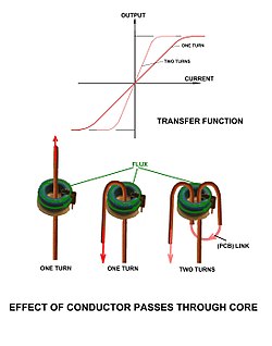
Ferrite toroid Hall effect current transducer[]

Hall sensors can detect stray magnetic fields easily, including that of Earth, so they work well as electronic compasses: but this also means that such stray fields can hinder accurate measurements of small magnetic fields. To solve this problem, Hall sensors are often integrated with magnetic shielding of some kind. For example, a Hall sensor integrated into a ferrite ring (as shown) can reduce the detection of stray fields by a factor of 100 or better (as the external magnetic fields cancel across the ring, giving no residual magnetic flux). This configuration also provides an improvement in signal-to-noise ratio and drift effects of over 20 times that of a bare Hall device.
The range of a given feedthrough sensor may be extended upward and downward by appropriate wiring. To extend the range to lower currents, multiple turns of the current-carrying wire may be made through the opening, each turn adding to the sensor output the same quantity; when the sensor is installed onto a printed circuit board, the turns can be carried out by a staple on the board. To extend the range to higher currents, a current divider may be used. The divider splits the current across two wires of differing widths and the thinner wire, carrying a smaller proportion of the total current, passes through the sensor.
Split ring clamp-on sensor[]
A variation on the ring sensor uses a split sensor which is clamped onto the line enabling the device to be used in temporary test equipment. If used in a permanent installation, a split sensor allows the electric current to be tested without dismantling the existing circuit.
Analog multiplication[]
The output is proportional to both the applied magnetic field and the applied sensor voltage. If the magnetic field is applied by a solenoid, the sensor output is proportional to the product of the current through the solenoid and the sensor voltage. As most applications requiring computation are now performed by small digital computers, the remaining useful application is in power sensing, which combines current sensing with voltage sensing in a single Hall effect device.
Power measurement[]
By sensing the current provided to a load and using the device's applied voltage as a sensor voltage it is possible to determine the power dissipated by a device.
Position and motion sensing[]
Hall effect devices used in motion sensing and motion limit switches can offer enhanced reliability in extreme environments. As there are no moving parts involved within the sensor or magnet, typical life expectancy is improved compared to traditional electromechanical switches. Additionally, the sensor and magnet may be encapsulated in an appropriate protective material. This application is used in brushless DC motors.
Hall effect sensors, affixed to mechanical gauges that have magnetized indicator needles, can translate the physical position or orientation of the mechanical indicator needle into an electrical signal that can be used by electronic indicators, controls or communications devices.[19]
Automotive ignition and fuel injection[]
Commonly used in distributors for ignition timing (and in some types of crank and camshaft position sensors for injection pulse timing, speed sensing, etc.) the Hall effect sensor is used as a direct replacement for the mechanical breaker points used in earlier automotive applications. Its use as an ignition timing device in various distributor types is as follows. A stationary permanent magnet and semiconductor Hall effect chip are mounted next to each other separated by an air gap, forming the Hall effect sensor. A metal rotor consisting of windows and tabs is mounted to a shaft and arranged so that during shaft rotation, the windows and tabs pass through the air gap between the permanent magnet and semiconductor Hall chip. This effectively shields and exposes the Hall chip to the permanent magnet's field respective to whether a tab or window is passing through the Hall sensor. For ignition timing purposes, the metal rotor will have a number of equal-sized tabs and windows matching the number of engine cylinders. This produces a uniform square wave output since the on/off (shielding and exposure) time is equal. This signal is used by the engine computer or ECU to control ignition timing. Many automotive Hall effect sensors have a built-in internal NPN transistor with an open collector and grounded emitter, meaning that rather than a voltage being produced at the Hall sensor signal output wire, the transistor is turned on providing a circuit to ground through the signal output wire.
Wheel rotation sensing[]
The sensing of wheel rotation is especially useful in anti-lock braking systems. The principles of such systems have been extended and refined to offer more than anti-skid functions, now providing extended vehicle handling enhancements.
Electric motor control[]
Some types of brushless DC electric motors use Hall effect sensors to detect the position of the rotor and feed that information to the motor controller. This allows for more precise motor control.
Industrial applications[]
Applications for Hall effect sensing have also expanded to industrial applications, which now use Hall effect joysticks to control hydraulic valves, replacing the traditional mechanical levers with contactless sensing. Such applications include mining trucks, backhoe loaders, cranes, diggers, scissor lifts, etc.
Spacecraft propulsion[]
A Hall-effect thruster (HET) is a device that is used to propel some spacecraft, after it gets into orbit or farther out into space. In the HET, atoms are ionized and accelerated by an electric field. A radial magnetic field established by magnets on the thruster is used to trap electrons which then orbit and create an electric field due to the Hall effect. A large potential is established between the end of the thruster where neutral propellant is fed, and the part where electrons are produced; so, electrons trapped in the magnetic field cannot drop to the lower potential. They are thus extremely energetic, which means that they can ionize neutral atoms. Neutral propellant is pumped into the chamber and is ionized by the trapped electrons. Positive ions and electrons are then ejected from the thruster as a quasineutral plasma, creating thrust. The thrust produced is extremely small, with a very low mass flow rate and a very high effective exhaust velocity/specific impulse. This is achieved at the cost of very high electrical power requirements, on the order of 4 KW for a few hundred millinewtons of thrust.
The Corbino effect[]

The Corbino effect is a phenomenon involving the Hall effect, but a disc-shaped metal sample is used in place of a rectangular one. Because of its shape the Corbino disc allows the observation of Hall effect–based magnetoresistance without the associated Hall voltage.
A radial current through a circular disc, subjected to a magnetic field perpendicular to the plane of the disc, produces a "circular" current through the disc.[20]
The absence of the free transverse boundaries renders the interpretation of the Corbino effect simpler than that of the Hall effect.
See also[]
- Capacitor
- Transducer
- Coulomb potential between two current loops embedded in a magnetic field
- Eddy current
- Eric Fawcett
- List of plasma (physics) articles
- Nernst effect
- Quantum Hall effect
- Fractional quantum Hall effect
- Quantum anomalous Hall effect
- Senftleben–Beenakker effect
- Spin Hall effect
- Thermal Hall effect
References[]
- ^ Edwin Hall (1879). "On a New Action of the Magnet on Electric Currents". American Journal of Mathematics. 2 (3): 287–92. doi:10.2307/2369245. JSTOR 2369245. Archived from the original on 2011-07-27. Retrieved 2008-02-28.
- ^ "Hall effect | Definition & Facts". Encyclopedia Britannica. Retrieved 2020-02-13.
- ^ Jump up to: a b Mani, R. G.; von Klitzing, K. (1994-03-07). "Hall effect under null current conditions". Applied Physics Letters. 64 (10): 1262–1264. doi:10.1063/1.110859. ISSN 0003-6951.
- ^ Bridgeman, P. W. (1939). Biographical Memoir of Edwin Herbert Hall. National Academy of Sciences.
- ^ Hall, E. H. (1879). "On a New Action of the Magnet on Electric Currents". American Journal of Mathematics. JSTOR. 2 (3): 287. doi:10.2307/2369245. ISSN 0002-9327.
- ^ "Hall Effect History". Archived from the original on 29 May 2015. Retrieved 2015-07-26.
- ^ Ramsden, Edward (2006). Hall-Effect Sensors. Elsevier Inc. pp. xi. ISBN 978-0-7506-7934-3.
- ^ "The Hall Effect". NIST. Archived from the original on 2008-03-07. Retrieved 2008-02-28.
- ^ "Hall Effect Sensor". Electronic Tutorials.
- ^ N.W. Ashcroft and N.D. Mermin "Solid State Physics" ISBN 978-0-03-083993-1
- ^ Ohgaki, Takeshi; Ohashi, Naoki; Sugimura, Shigeaki; Ryoken, Haruki; Sakaguchi, Isao; Adachi, Yutaka; Haneda, Hajime (2008). "Positive Hall coefficients obtained from contact misplacement on evident n-type ZnO films and crystals". Journal of Materials Research. 23 (9): 2293. Bibcode:2008JMatR..23.2293O. doi:10.1557/JMR.2008.0300.
- ^ Kasap, Safa. "Hall Effect in Semiconductors" (PDF). Archived from the original (PDF) on 2008-08-21.
- ^ "Hall Effect". hyperphysics.phy-astr.gsu.edu. Retrieved 2020-02-13.
- ^ Mark Wardle (2004). "Star Formation and the Hall Effect". Astrophysics and Space Science. 292 (1): 317–323. arXiv:astro-ph/0307086. Bibcode:2004Ap&SS.292..317W. CiteSeerX 10.1.1.746.8082. doi:10.1023/B:ASTR.0000045033.80068.1f.
- ^ Braiding, C. R.; Wardle, M. (2012). "The Hall effect in star formation". Monthly Notices of the Royal Astronomical Society. 422 (1): 261. arXiv:1109.1370. Bibcode:2012MNRAS.422..261B. doi:10.1111/j.1365-2966.2012.20601.x.
- ^ Braiding, C. R.; Wardle, M. (2012). "The Hall effect in accretion flows". Monthly Notices of the Royal Astronomical Society. 427 (4): 3188. arXiv:1208.5887. Bibcode:2012MNRAS.427.3188B. doi:10.1111/j.1365-2966.2012.22001.x.
- ^ Robert Karplus and J. M. Luttinger (1954). "Hall Effect in Ferromagnetics". Phys. Rev. 95 (5): 1154–1160. Bibcode:1954PhRv...95.1154K. doi:10.1103/PhysRev.95.1154.
- ^ N. A. Sinitsyn (2008). "Semiclassical Theories of the Anomalous Hall Effect". Journal of Physics: Condensed Matter. 20 (2): 023201. arXiv:0712.0183. Bibcode:2008JPCM...20b3201S. doi:10.1088/0953-8984/20/02/023201.
- ^ Tank Sensors & Probes, Electronic Sensors, Inc., retrieved August 8, 2018
- ^ Adams, E. P. (1915). The Hall and Corbino effects. Proceedings of the American Philosophical Society. 54. pp. 47–51. Bibcode:1916PhDT.........2C. ISBN 978-1-4223-7256-2. Retrieved 2009-01-24.
Sources[]
- Introduction to Plasma Physics and Controlled Fusion, Volume 1, Plasma Physics, Second Edition, 1984, Francis F. Chen
Further reading[]
- Baumgartner, A.; Ihn, T.; Ensslin, K.; Papp, G.; Peeters, F.; Maranowski, K.; Gossard, A. C. (2006). "Classical Hall effect in scanning gate experiments". Physical Review B. 74 (16). Bibcode:2006PhRvB..74p5426B. doi:10.1103/PhysRevB.74.165426. hdl:10067/613600151162165141.
- Annraoi M. de Paor. Correction to the classical two-species Hall Coefficient using twoport network theory. International Journal of Electrical Engineering Education 43/4.
- NIST The Hall Effect
- University of Washington The Hall Effect
External links[]
- Patents
- U.S. Patent 1,778,796, P. H. Craig, System and apparatus employing the Hall effect
- U.S. Patent 3,596,114, J. T. Maupin, E. A. Vorthmann, Hall effect contactless switch with prebiased Schmitt trigger
- US Patent 5646527, R. G. Mani & K. von Klitzing, "Hall-effect device with current and Hall-voltage connections"
- General
- Understanding and Applying the Hall Effect
- Hall Effect Thrusters Alta Space
- Hall effect calculators
- Interactive Java tutorial on the Hall effect National High Magnetic Field Laboratory
- Science World (wolfram.com) article.
- "The Hall Effect". nist.gov.
- Table with Hall coefficients of different elements at room temperature.
- Simulation of the Hall effect as a Youtube video
- Hall effect in electrolytes
- Bowley, Roger (2010). "Hall Effect". Sixty Symbols. Brady Haran for the University of Nottingham.
| show Condensed matter physics |
|---|

| show Authority control |
|---|
- Hall effect
- Condensed matter physics
- Electric and magnetic fields in matter