Apple A9
 Apple A9 processor | |
| General information | |
|---|---|
| Launched | September 9, 2015 |
| Discontinued | September 12, 2018 |
| Designed by | Apple Inc. |
| Common manufacturer(s) |
|
| Product code | APL0898,[1] APL1022[2] |
| Performance | |
| Max. CPU clock rate | 1.85 GHz (iPhone 6s, iPhone 6s Plus, iPhone SE, iPad 9.7 2017)[3][4] |
| Cache | |
| L1 cache | Per core: 64 KB instruction + 64 KB data |
| L2 cache | 3 MB shared[5] |
| L3 cache | 4 MB shared[6] |
| Architecture and classification | |
| Application | Mobile |
| Min. feature size | 16 nm (TSMC) to 14 nm (Samsung) |
| Microarchitecture | Twister[7][8] |
| Instruction set | ARMv8-A: A64, A32, T32 |
| Physical specifications | |
| Cores |
|
| GPU(s) | Custom PowerVR Series 7XT (six-core) @ 650MHz [9][10][11] |
| Products, models, variants | |
| Variant(s) |
|
| History | |
| Predecessor | Apple A8 |
| Successor | Apple A10 Fusion |
The Apple A9 is a 64-bit ARM-based system-on-chip (SoC), designed by Apple Inc. Manufactured for Apple by both TSMC and Samsung, it first appeared in the iPhone 6S and 6S Plus which were introduced on September 9, 2015.[12] Apple states that it has 70% more CPU performance and 90% more graphics performance compared to its predecessor, the Apple A8.[12]
Design[]
The A9 features an Apple-designed 64-bit 1.85 GHz[3] ARMv8-A dual-core[5] CPU called Twister.[8] The A9 in the iPhone 6S has 2 GB of LPDDR4 RAM included in the package.[1][5] The A9 has a per-core L1 cache of 64 KB for data and 64 KB for instructions, an L2 cache of 3 MB shared by both CPU cores, and a 4 MB L3 cache that services the entire SoC and acts as a victim cache.[6] The A9 also features a custom PowerVR Series7XT @ 650 MHz GPU, featuring 6x custom shader cores and compiler from Apple.[13]
The A9 includes a new image processor, a feature originally introduced in the A5 and last updated in the A7, with better temporal and spatial noise reduction as well as improved local tone mapping.[14] The A9 directly integrates an embedded M9 motion coprocessor, a feature originally introduced with the A7 as a separate chip. In addition to servicing the accelerometer, gyroscope, compass, and barometer, the M9 coprocessor can recognize Siri voice commands.[14] The A9 adds hardware decoding for HEIF and 8-bit and 10-bit HEVC.[15]
The A9 features a custom storage solution, which uses an Apple-designed NVMe-based controller that communicates over a PCIe connection.[16] The iPhone 6s' NAND design is more akin to a PC-class SSD than embedded flash memory common on mobile devices. This gives the phone a significant storage performance advantage over competitors which often use eMMC or UFS to connect to their flash memory.
Microarchitecture[]
The A9's microarchitecture is similar to the second generation Cyclone (used in A8 chip) microarchitecture. Some of the microarchitectural features are as follows:
| Pipeline depth (stages) | 16 |
|---|---|
| Issue width | 6 micro-ops |
| ROB | 196 micro-ops |
| Load latency | 8 cycles |
| Branch misprediction penalty | 9 |
| Number of integer pipes | 4 |
| Number of shifter ALUs | 4 |
| Load/Store Units | 2 |
| Integer pipe buffer size | 48 |
| Number of branch units | 2 |
| Indirect branch units | 1 |
| Branch pipe buffer size | 24 |
| FP ALUs | 3 |
About half of the performance boost over A8 comes from the 1.85 GHz frequency. About a quarter comes from the better memory subsystem (3× bigger caches). The remaining quarter comes from the microarchitectural tuning and smaller technology node.[citation needed]
Encryption[]
According to Apple, "Every iOS device has a dedicated AES-256 crypto engine built into the DMA path between the flash storage and main system memory, making file encryption highly efficient. On A9 or later A-series processors, the flash storage subsystem is on an isolated bus that is only granted access to memory containing user data via the DMA crypto engine."[17]
Dual sourcing[]
Apple A9 chips are fabricated by two companies: Samsung and TSMC. The Samsung version is called APL0898, which is manufactured on a 14 nm FinFET process and is 96 mm2 large, while the TSMC version is called APL1022, which is manufactured on a 16 nm FinFET process and is 104.5 mm2 large.
There was intended to be no significant difference in performance between the parts,[18] but in October 2015, it was alleged that iPhone 6S models with Samsung-fabricated A9 chips consistently measured shorter battery life than those with TSMC-fabricated versions in CPU heavy usage; web browsing and graphics were not very different.[19] Apple responded that "tests which run the processors with a continuous heavy workload until the battery depletes are not representative of real-world usage", and said that internal testing combined with customer data demonstrated a variance of only 2–3%.[20][21]
Naming[]
While the Twister CPU core implements the ARMv8-A instruction set architecture licensed from ARM Holdings, it is an independent CPU design and is unrelated to the much older but similarly named Cortex-A9 and ARM9 CPU that are designed by ARM themselves and implement the 32-bit ARMv7-A and ARMv5E versions of the architecture.
Gallery[]
The processors are nearly identical visually. The packaging have the same dimensions (approx 15.0×14.5 mm) and only superficial differences, like the designation text. Inside the packaging the silicon die differs in size.
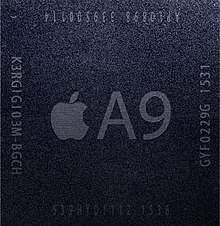
APL0898, the Samsung version of the A9.

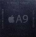
APL1022, the TSMC version of the A9.
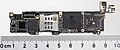
A9 (APL0898) SoC on iPhone 6s main logic board.
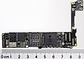
A9 (APL1022) SoC on iPhone SE main logic board.


ARKit[]
The A9 processor is listed as the minimum requirement for ARKit. [22]
Products that include the Apple A9[]
- iPhone 6S and 6S Plus
- iPhone SE (1st generation)
- iPad (5th generation)
See also[]
- Apple silicon, the range of ARM-based processors designed by Apple.
- Apple A9X
References[]
- ^ Jump up to: a b "iPhone 6s Teardown". iFixit. September 25, 2015. Retrieved September 26, 2015.
- ^ "A9 is TSMC 16nm FinFET and Samsung Fabbed". Archived from the original on 2016-09-17. Retrieved 2015-09-28.
- ^ Jump up to: a b "iPhone 6s customer receives her device early, benchmarks show a marked increase in power". iDownloadBlog. September 21, 2015. Retrieved September 25, 2015.
- ^ "Revealed: iPhone 6S uses 1.85GHz dual-core A9 chip". Trusted Reviews. September 18, 2015. Retrieved September 25, 2015.
- ^ Jump up to: a b c d "Inside the iPhone 6s". Chipworks. September 25, 2015. Archived from the original on February 3, 2017. Retrieved September 26, 2015.
- ^ Jump up to: a b Smith, Ryan (November 30, 2015). "Correcting Apple's A9 SoC L3 Cache Size: A 4MB Victim Cache". AnandTech. Retrieved 1 December 2015.
- ^ Joshua Ho. "iPhone 6s and iPhone 6s Plus Preliminary Results".
- ^ Jump up to: a b Joshua Ho, Ryan Smith. "A9's CPU: Twister - The Apple iPhone 6s and iPhone 6s Plus Review".
- ^ "iPhone 6S Review". GSM Arena. October 2015.
- ^ "Apple A9 / PowerVR GT7600". NotebookCheck. September 2015.
- ^ Kanter, David. "A Look Inside Apple's Custom GPU for the iPhone". Retrieved 2019-08-27.
- ^ Jump up to: a b "Apple Introduces iPhone 6s & iPhone 6s Plus" (Press release). Apple. September 9, 2015. Retrieved September 9, 2015.
- ^ Kanter, David. "A Look Inside Apple's Custom GPU for the iPhone". Retrieved 2019-08-27.
- ^ Jump up to: a b "iPhone 6s - Technology". Apple. September 8, 2015. Retrieved September 10, 2015.
- ^ Apple has chosen HEVC as its next-generation video codec. 8 June 2017.
- ^ "The Apple iPhone 6s and iPhone 6s Plus Review". Anandtech. November 2, 2015. Retrieved April 4, 2016.
- ^ iOS Security, January 2018, https://www.apple.com/business/docs/iOS_Security_Guide.pdf
- ^ Smith, Ryan (September 28, 2015). "Apple's A9 SoC Is Dual Sourced From Samsung & TSMC". AnandTech. Retrieved 30 September 2015.
- ^ Cunningham, Andrew (12 October 2015). "Samsung vs. TSMC: Comparing the battery life of two Apple A9s". Ars Technica. Condé Nast. Retrieved 13 October 2015.
- ^ "Analyzing Apple's Statement on TSMC and Samsung A9 SoCs". AnandTech. Retrieved 11 October 2015.
- ^ Barrett, Brian. "It Doesn't Matter Which A9 Chip Your iPhone Has. Get Over It". Wired. Retrieved 11 October 2015.
- ^ "Framework - ARKit". Retrieved 4 Aug 2017.
| show Apple Inc. |
|---|
- Apple Inc. mobile processors
- ARM architecture
- Computer-related introductions in 2015