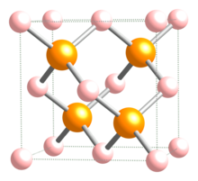
Indium phosphide
| |
| |
| Names | |
|---|---|
| Other names
Indium(III) phosphide
| |
| Identifiers | |
3D model (JSmol)
|
|
| ChemSpider | |
| ECHA InfoCard | 100.040.856 |
PubChem CID
|
|
| UNII | |
CompTox Dashboard (EPA)
|
|
| Properties | |
| InP | |
| Molar mass | 145.792 g/mol |
| Appearance | black cubic crystals |
| Density | 4.81 g/cm3, solid |
| Melting point | 1,062 °C (1,944 °F; 1,335 K) |
| Solubility | slightly soluble in acids[1] |
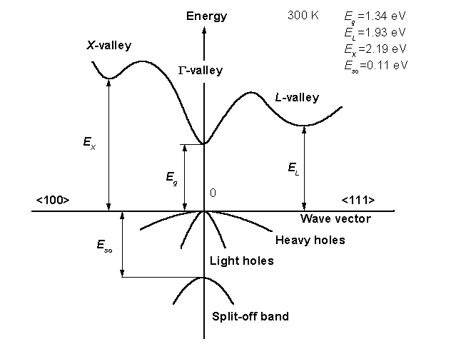
| Band gap | 1.344 eV (300 K; direct) |
| Electron mobility | 5400 cm2/(V·s) (300 K) |
| Thermal conductivity | 0.68 W/(cm·K) (300 K) |
Refractive index (nD)
|
3.1 (infrared); 3.55 (632.8 nm)[2] |
| Structure | |
| Zinc blende | |
a = 5.8687 Å [3]
| |
| Tetrahedral | |
| Thermochemistry | |
Heat capacity (C)
|
45.4 J/(mol·K)[4] |
Std molar
entropy (S |
59.8 J/(mol·K) |
Std enthalpy of
formation (ΔfH⦵298) |
-88.7 kJ/mol |
| Hazards | |
| Main hazards | Toxic, hydrolysis to phosphine |
| Safety data sheet | External MSDS |
| Related compounds | |
Other anions
|
Indium nitride Indium arsenide Indium antimonide |
Other cations
|
Aluminium phosphide Gallium phosphide |
Related compounds
|
Indium gallium phosphide Aluminium gallium indium phosphide Gallium indium arsenide antimonide phosphide |
Except where otherwise noted, data are given for materials in their standard state (at 25 °C [77 °F], 100 kPa). | |
| Infobox references | |
Indium phosphide (InP) is a binary semiconductor composed of indium and phosphorus. It has a face-centered cubic ("zincblende") crystal structure, identical to that of GaAs and most of the III-V semiconductors.
Manufacturing[]

Indium phosphide can be prepared from the reaction of white phosphorus and indium iodide[clarification needed] at 400 °C.,[5] also by direct combination of the purified elements at high temperature and pressure, or by thermal decomposition of a mixture of a trialkyl indium compound and phosphine.[6]
Uses[]
InP is used in high-power and high-frequency electronics[citation needed] because of its superior electron velocity with respect to the more common semiconductors silicon and gallium arsenide.
It was used with indium gallium arsenide to make a record breaking pseudomorphic heterojunction bipolar transistor that could operate at 604 GHz.[7]
It also has a direct bandgap, making it useful for optoelectronics devices like laser diodes. The company Infinera uses indium phosphide as its major technological material for manufacturing photonic integrated circuits for the optical telecommunications industry, to enable wavelength-division multiplexing[8] applications.
InP is also used as a substrate for epitaxial indium gallium arsenide based opto-electronic devices.
Applications[]
This section does not cite any sources. (April 2020) |
The application fields of InP splits up into three main areas. It is used as the basis
- for optoelectronic components
- for high-speed electronics.
- for photovoltaics
There is still a vastly under-utilized, yet technically exciting zone in the electromagnetic spectrum between microwaves and infrared, often referred to as “Terahertz”. Electromagnetic waves in this range possess hybrid properties they show high-frequency- and optical characteristics simultaneously. InP based components unlock this spectral range for important new applications.
Optoelectronic Applications[]
InP based lasers and LEDs can emit light in the very broad range of 1200 nm up to 12 µm. This light is used for fibre based Telecom and Datacom applications in all areas of the digitalised world. Light is also used for sensing applications. On one hand there are spectroscopic applications, where a certain wavelength is needed to interact with matter to detect highly diluted gases for example. Optoelectronic terahertz is used in ultra-sensitive spectroscopic analysers, thickness measurements of polymers and for the detection of multilayer coatings in the automotive industry. On the other hand there is a huge benefit of specific InP lasers because they are eye safe. The radiation is absorbed in the vitreous body of the human eye and cannot harm the retina.
Telecom/Datacom[]
Indium Phosphide (InP) is used to produce efficient lasers, sensitive photodetectors and modulators in the wavelength window typically used for telecommunications, i.e., 1550 nm wavelengths, as it is a direct bandgap III-V compound semiconductor material. The wavelength between about 1510 nm and 1600 nm has the lowest attenuation available on optical fibre (about 0.26 dB/km). InP is a commonly used material for the generation of laser signals and the detection and conversion of those signals back to electronic form. Wafer diameters range from 2-4 inches.
Applications are:
• Long-haul optical fibre connections over great distance up to 5000 km typically >10 Tbit/s
• Metro ring access networks
• Company networks and data center
• Fibre to the home
• Connections to wireless 3G, LTE and 5G base stations
• Free space satellite communication
Optical Sensing[]
Spectroscopic Sensing aiming environmental protection and identification of dangerous substances
• A growing field is sensing based on the wavelength regime of InP. One example for Gas Spectroscopy is drive test equipment with real-time measurement of (CO, CO2, NOX [or NO + NO2]).
• Another example is FT-IR-Spectrometer VERTEX with a terahertz source. The terahertz radiation is generated from the beating signal of 2 InP lasers and an InP antenna that transforms the optical signal to the terahertz regime.
• Stand-Off detection of traces of explosive substances on surfaces, e.g. for safety applications on airports or crime scene investigation after assassination attempts.
• Quick verification of traces of toxic substances in gases and liquids (including tap water) or surface contaminations down to the ppb level.
• Spectroscopy for non-destructive product control of e.g. food (early detection of spoiled foodstuff)
• Spectroscopy for many novel applications, especially in air pollution control are being discussed today and implementations are on the way.
LiDAR systems for the automotive sector and industry 4.0[]
Widely discussed in the LiDAR arena is the wavelength of the signal. While some players have opted for 830-to-940-nm wavelengths to take advantage of available optical components, companies (including Blackmore, Neptec, Aeye, and ) are increasingly turning to longer wavelengths in the also-well-served 1550-nm wavelength band, as those wavelengths allow laser powers roughly 100 times higher to be employed without compromising public safety. Lasers with emission wavelengths longer than ≈ 1.4 μm are often called “eye-safe” because light in that wavelength range is strongly absorbed in the eye's cornea, lens and vitreous body and therefore cannot damage the sensitive retina).
• LiDAR-based sensor technology can provide a high level of object identification and classification with three-dimensional (3D) imaging techniques.
• The automotive industry will adopt a chip-based, low cost solid state LiDAR sensor technology instead of large, expensive, mechanical LiDAR systems in the future.
• For the most advanced chip-based LiDAR systems, InP will play an important role and will enable autonomous driving. (Report: Blistering Growth for Automotive Lidar, Stewart Wills). The longer eye safe wavelength is also more appropriate dealing with real world conditions like dust, fog and rain.
High-speed electronics[]
Today's semiconductor technology allows the creation and detection of very high frequencies of 100 GHz and higher. Such components find their applications in wireless high-speed data communication (directional radio), radars (compact, energy-efficient and highly resolving), and radiometric sensing e. g. for weather- or atmospheric observations.
InP is also used to realize high-speed microelectronics and such semiconductor devices are the fastest devices available today. Typically, microelectronics on InP is based on High Electron Mobility Transistors (HEMT) or on Heterostructure Bipolar Transistors (HBT). The sizes and volumes of both transistors based on InP material is very small: 0.1 µm x 10 µm x 1 µm. Typical substrate thicknesses are < 100 µm. These transistors are assembled into circuits and modules for the following applications:
• Security scanning systems: Imaging systems for airport security imaging and scanners for civil security applications
• Wireless communications: High-speed 5G wireless communications will explore InP technology due to its superior performance. Such systems operate at frequencies beyond 100 GHz in order to support high data rates
• Biomedical applications: Millimeter-wave and THz spectrometers are employed for non-invasive diagnostics in medical applications from cancer tissue identification, diabetes detection, to medical diagnostics using human exhaled air.
• Non-destructive testing: Industrial applications employ scanning systems for quality control in e.g. automotive paint thickness applications and defects in composite materials in aerospace
• Robotics: Robotic vision is essentially based on high resolution imaging radar systems at millimetre-waves
• Radiometric sensing: Almost all components and pollutions in the atmosphere show characteristic absorptions/emissions (fingerprints) in the microwave range. InP allows to fabricate small, lightweight and mobile systems to identify such substances.
Photovoltaic applications[]
Photovoltaic cells with highest efficiencies of up to 46% (Press Release, Fraunhofer ISE, 1. December 2014) implement InP substrates to achieve an optimal bandgap combination to efficiently convert solar radiation into electrical energy. Today, only InP substrates achieve the lattice constant to grow the required low bandgap materials with high crystalline quality. Research groups all over the world are looking for replacements due to the high costs of these materials. However, up to now all other options yield lower material qualities and hence lower conversion efficiencies. Further research focusses on the re-use of the InP substrate as template for the production of further solar cells.
Also today’s state-of-the-art high-efficiency solar cells for concentrator photovoltaics (CPV) and for space applications use (Ga)InP and other III-V compounds to achieve the required bandgap combinations. Other technologies, such as Si solar cells, provide only half the power than III-V cells and furthermore show much stronger degradation in the harsh space environment. Finally, Si-based solar cells are also much heavier than III-V solar cells and yield to a higher amount of space debris. One way to significantly increase conversion efficiency also in terrestrial PV systems is the use of similar III-V solar cells in CPV systems where only about one-tenth of a percent of the area is covered by high-efficiency III-V solar cells.
Chemistry[]
Indium phosphide also has one of the longest-lived optical phonons of any compound with the zincblende crystal structure.[9][10]
References[]
- ^ Lide, David R. (1998), Handbook of Chemistry and Physics (87 ed.), Boca Raton, Florida: CRC Press, pp. 4–61, ISBN 0-8493-0594-2
- ^ Sheng Chao, Tien; Lee, Chung Len; Lei, Tan Fu (1993), "The refractive index of InP and its oxide measured by multiple-angle incident ellipsometry", Journal of Materials Science Letters, 12 (10): 721, doi:10.1007/BF00626698.
- ^ "Basic Parameters of InP".
- ^ Lide, David R. (1998), Handbook of Chemistry and Physics (87 ed.), Boca Raton, Florida: CRC Press, pp. 5–20, ISBN 0-8493-0594-2
- ^ Indium Phosphide at HSDB
- ^ InP manufacture
- ^ Indium Phosphide and Indium Gallium Arsenide Help Break 600 Gigahertz Speed Barrier. April 2005
- ^ The Light Brigade appeared in Red Herring in 2002. Archived June 7, 2011, at the Wayback Machine
- ^ Bouarissa, Nadir (July 2011). "Phonons and related crystal properties in indium phosphide under pressure". Physica B: Condensed Matter. 406 (13): 2583–2587. Bibcode:2011PhyB..406.2583B. doi:10.1016/j.physb.2011.03.073.
- ^ Degheidy, Abdel Razik; Elkenany, Elkenany Brens; Madkour, Mohamed Abdel Kader; Abuali, Ahmed. M. (2018-09-01). "Temperature dependence of phonons and related crystal properties in InAs, InP and InSb zinc-blende binary compounds". Computational Condensed Matter. 16: e00308. doi:10.1016/j.cocom.2018.e00308.
External links[]
- Phosphides
- Indium compounds
- Inorganic phosphorus compounds
- Optoelectronics
- III-V semiconductors
- III-V compounds
- IARC Group 2A carcinogens
- Zincblende crystal structure