Intel 8086
 A rare Intel C8086 processor in purple ceramic DIP package with side-brazed pins | |
| General information | |
|---|---|
| Launched | 1978 |
| Discontinued | 1998[1] |
| Common manufacturer(s) |
|
| Performance | |
| Max. CPU clock rate | 5 MHz to 10 MHz |
| Data width | 16 bits |
| Address width | 20 bits |
| Architecture and classification | |
| Min. feature size | 3 µm |
| Instruction set | x86-16 |
| Physical specifications | |
| Transistors |
|
| Co-processor | Intel 8087, Intel 8089 |
| Package(s) |
|
| Socket(s) | |
| Products, models, variants | |
| Variant(s) | |
| History | |
| Predecessor | Intel 8085 |
| Successor | 80186 and 80286 (both of which were introduced in early 1982) |
The 8086[2] (also called iAPX 86)[3] is a 16-bit microprocessor chip designed by Intel between early 1976 and June 8, 1978, when it was released. The Intel 8088, released July 1, 1979,[4] is a slightly modified chip with an external 8-bit data bus (allowing the use of cheaper and fewer supporting ICs),[note 1] and is notable as the processor used in the original IBM PC design.
The 8086 gave rise to the x86 architecture, which eventually became Intel's most successful line of processors. On June 5, 2018, Intel released a limited-edition CPU celebrating the 40th anniversary of the Intel 8086, called the Intel Core i7-8086K.[4]
History[]
Background[]
In 1972, Intel launched the 8008, the first 8-bit microprocessor.[note 2] It implemented an instruction set designed by Datapoint corporation with programmable CRT terminals in mind, which also proved to be fairly general-purpose. The device needed several additional ICs to produce a functional computer, in part due to it being packaged in a small 18-pin "memory package", which ruled out the use of a separate address bus (Intel was primarily a DRAM manufacturer at the time).
Two years later, Intel launched the 8080,[note 3] employing the new 40-pin DIL packages originally developed for calculator ICs to enable a separate address bus. It has an extended instruction set that is source-compatible (not binary compatible) with the 8008[5] and also includes some 16-bit instructions to make programming easier. The 8080 device was eventually replaced by the depletion-load-based 8085 (1977), which sufficed with a single +5 V power supply instead of the three different operating voltages of earlier chips.[note 4] Other well known 8-bit microprocessors that emerged during these years are Motorola 6800 (1974), General Instrument PIC16X (1975), MOS Technology 6502 (1975), Zilog Z80 (1976), and Motorola 6809 (1978).
The first x86 design[]

The 8086 project started in May 1976 and was originally intended as a temporary substitute for the ambitious and delayed iAPX 432 project. It was an attempt to draw attention from the less-delayed 16- and 32-bit processors of other manufacturers (such as Motorola, Zilog, and National Semiconductor) and at the same time to counter the threat from the Zilog Z80 (designed by former Intel employees), which became very successful. Both the architecture and the physical chip were therefore developed rather quickly by a small group of people, and using the same basic microarchitecture elements and physical implementation techniques as employed for the slightly older 8085 (and for which the 8086 also would function as a continuation).
Marketed as source compatible,[6] the 8086 was designed to allow assembly language for the 8008[citation needed], 8080, or 8085 to be automatically converted into equivalent (suboptimal) 8086 source code, with little or no hand-editing. The programming model and instruction set is (loosely) based on the 8080 in order to make this possible. However, the 8086 design was expanded to support full 16-bit processing.
New kinds of instructions were added as well; full support for signed integers, base+offset addressing, and self-repeating operations were akin to the Z80 design[7] but were all made slightly more general in the 8086. Instructions directly supporting nested ALGOL-family languages such as Pascal and PL/M were also added. According to principal architect Stephen P. Morse, this was a result of a more software-centric approach than in the design of earlier Intel processors (the designers had experience working with compiler implementations). Other enhancements included microcoded multiply and divide instructions and a bus structure better adapted to future coprocessors (such as 8087 and 8089) and multiprocessor systems.
The first revision of the instruction set and high level architecture was ready after about three months,[note 5] and as almost no CAD tools were used, four engineers and 12 layout people were simultaneously working on the chip.[note 6] The 8086 took a little more than two years from idea to working product, which was considered rather fast for a complex design in 1976–1978.
The 8086 was sequenced[note 7] using a mixture of random logic[8] and microcode and was implemented using depletion-load nMOS circuitry with approximately 20,000 active transistors (29,000 counting all ROM and PLA sites). It was soon moved to a new refined nMOS manufacturing process called HMOS (for High performance MOS) that Intel originally developed for manufacturing of fast static RAM products.[note 8] This was followed by HMOS-II, HMOS-III versions, and, eventually, a fully static CMOS version for battery powered devices, manufactured using Intel's CHMOS processes.[note 9] The original chip measured 33 mm² and minimum feature size was 3.2 μm.
The architecture was defined by Stephen P. Morse with some help from Bruce Ravenel (the architect of the 8087) in refining the final revisions. Logic designer Jim McKevitt and John Bayliss were the lead engineers of the hardware-level development team[note 10] and Bill Pohlman the manager for the project. The legacy of the 8086 is enduring in the basic instruction set of today's personal computers and servers; the 8086 also lent its last two digits to later extended versions of the design, such as the Intel 286 and the Intel 386, all of which eventually became known as the x86 family. (Another reference is that the PCI Vendor ID for Intel devices is 8086h.)
Details[]

Buses and operation[]
All internal registers, as well as internal and external data buses, are 16 bits wide, which firmly established the "16-bit microprocessor" identity of the 8086. A 20-bit external address bus provides a 1 MB physical address space (220 = 1,048,576). This address space is addressed by means of internal memory "segmentation". The data bus is multiplexed with the address bus in order to fit all of the control lines into a standard 40-pin dual in-line package. It provides a 16-bit I/O address bus, supporting 64 KB of separate I/O space. The maximum linear address space is limited to 64 KB, simply because internal address/index registers are only 16 bits wide. Programming over 64 KB memory boundaries involves adjusting the segment registers (see below); this difficulty existed until the 80386 architecture introduced wider (32-bit) registers (the memory management hardware in the 80286 did not help in this regard, as its registers are still only 16 bits wide).
Hardware modes[]
Some of the control pins, which carry essential signals for all external operations, have more than one function depending upon whether the device is operated in min or max mode. The former mode is intended for small single-processor systems, while the latter is for medium or large systems using more than one processor (a kind of multiprocessor mode). Maximum mode is required when using an 8087 or 8089 coprocessor. The voltage on pin 33 (MN/MX) determines the mode. Changing the state of pin 33 changes the function of certain other pins, most of which have to do with how the CPU handles the (local) bus.[note 11] The mode is usually hardwired into the circuit and therefore cannot be changed by software. The workings of these modes are described in terms of timing diagrams in Intel datasheets and manuals. In minimum mode, all control signals are generated by the 8086 itself.
Registers and instructions[]
| ||||||||||||||||||||||||||||||||||||||||||||||||||||||||||||||||||||||||||||||||||||||||||||||||||||||||||||||||||||||||||||||||||||||||||||||||||||||||||||||||||||||||||||||||||||||||||||||||||||||||||||||||||||||||||||||||||||||||||||||||||||||||||||||||||||||||||||||||||||||||||||||||||||||||||||||||||||||||||||||||||||||||||||||||||||||||||||||||||||||||||||||||||||||||||||||||||||||||||||||||||||||||||||||||||||
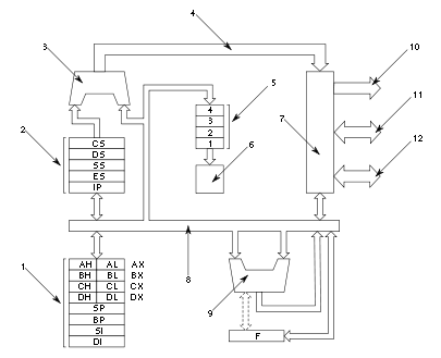
The 8086 has eight more or less general 16-bit registers (including the stack pointer but excluding the instruction pointer, flag register and segment registers). Four of them, AX, BX, CX, DX, can also be accessed as twice as many 8-bit registers (see figure) while the other four, SI, DI, BP, SP, are 16-bit only.
Due to a compact encoding inspired by 8-bit processors, most instructions are one-address or two-address operations, which means that the result is stored in one of the operands. At most one of the operands can be in memory, but this memory operand can also be the destination, while the other operand, the source, can be either register or immediate. A single memory location can also often be used as both source and destination which, among other factors, further contributes to a code density comparable to (and often better than) most eight-bit machines at the time.
The degree of generality of most registers is much greater than in the 8080 or 8085. However, 8086 registers were more specialized than in most contemporary minicomputers and are also used implicitly by some instructions. While perfectly sensible for the assembly programmer, this makes register allocation for compilers more complicated compared to more orthogonal 16-bit and 32-bit processors of the time such as the PDP-11, VAX, 68000, 32016, etc. On the other hand, being more regular than the rather minimalistic but ubiquitous 8-bit microprocessors such as the 6502, 6800, 6809, 8085, MCS-48, 8051, and other contemporary accumulator-based machines, it is significantly easier to construct an efficient code generator for the 8086 architecture.
Another factor for this is that the 8086 also introduced some new instructions (not present in the 8080 and 8085) to better support stack-based high-level programming languages such as Pascal and PL/M; some of the more useful instructions are push mem-op, and ret size, supporting the "Pascal calling convention" directly. (Several others, such as push immed and enter, were added in the subsequent 80186, 80286, and 80386 processors.)
A 64 KB (one segment) stack growing towards lower addresses is supported in hardware; 16-bit words are pushed onto the stack, and the top of the stack is pointed to by SS:SP. There are 256 interrupts, which can be invoked by both hardware and software. The interrupts can cascade, using the stack to store the return addresses.
The 8086 has 64 K of 8-bit (or alternatively 32 K of 16-bit word) I/O port space.
Flags[]
The 8086 has a 16-bit flags register. Nine of these condition code flags are active, and indicate the current state of the processor: Carry flag (CF), Parity flag (PF), Auxiliary carry flag (AF), Zero flag (ZF), Sign flag (SF), Trap flag (TF), Interrupt flag (IF), Direction flag (DF), and Overflow flag (OF). Also referred to as the status word, the layout of the flags register is as follows:[9]
| Bit | 15-12 | 11 | 10 | 9 | 8 | 7 | 6 | 5 | 4 | 3 | 2 | 1 | 0 |
|---|---|---|---|---|---|---|---|---|---|---|---|---|---|
| Flag | OF | DF | IF | TF | SF | ZF | AF | PF | CF |
Segmentation[]
There are also four 16-bit segment registers (see figure) that allow the 8086 CPU to access one megabyte of memory in an unusual way. Rather than concatenating the segment register with the address register, as in most processors whose address space exceeds their register size, the 8086 shifts the 16-bit segment only four bits left before adding it to the 16-bit offset (16×segment + offset), therefore producing a 20-bit external (or effective or physical) address from the 32-bit segment:offset pair. As a result, each external address can be referred to by 212 = 4096 different segment:offset pairs.
| 0110 1000 1000 0111 0000 | Segment, | 16 bits, shifted 4 bits left (or multiplied by 0x10) |
| + 0011 0100 1010 1001 | Offset, | 16 bits |
| 0110 1011 1101 0001 1001 | Address, | 20 bits |
Although considered complicated and cumbersome by many programmers, this scheme also has advantages; a small program (less than 64 KB) can be loaded starting at a fixed offset (such as 0000) in its own segment, avoiding the need for relocation, with at most 15 bytes of alignment waste.
Compilers for the 8086 family commonly support two types of pointer, near and far. Near pointers are 16-bit offsets implicitly associated with the program's code or data segment and so can be used only within parts of a program small enough to fit in one segment. Far pointers are 32-bit segment:offset pairs resolving to 20-bit external addresses. Some compilers also support huge pointers, which are like far pointers except that pointer arithmetic on a huge pointer treats it as a linear 20-bit pointer, while pointer arithmetic on a far pointer wraps around within its 16-bit offset without touching the segment part of the address.
To avoid the need to specify near and far on numerous pointers, data structures, and functions, compilers also support "memory models" which specify default pointer sizes. The tiny (max 64K), small (max 128K), compact (data > 64K), medium (code > 64K), large (code,data > 64K), and huge (individual arrays > 64K) models cover practical combinations of near, far, and huge pointers for code and data. The tiny model means that code and data are shared in a single segment, just as in most 8-bit based processors, and can be used to build .com files for instance. Precompiled libraries often come in several versions compiled for different memory models.
According to Morse et al.,.[10] the designers actually contemplated using an 8-bit shift (instead of 4-bit), in order to create a 16 MB physical address space. However, as this would have forced segments to begin on 256-byte boundaries, and 1 MB was considered very large for a microprocessor around 1976, the idea was dismissed. Also, there were not enough pins available on a low cost 40-pin package for the additional four address bus pins.
In principle, the address space of the x86 series could have been extended in later processors by increasing the shift value, as long as applications obtained their segments from the operating system and did not make assumptions about the equivalence of different segment:offset pairs.[note 12] In practice the use of "huge" pointers and similar mechanisms was widespread and the flat 32-bit addressing made possible with the 32-bit offset registers in the 80386 eventually extended the limited addressing range in a more general way (see below).
Intel could have decided to implement memory in 16 bit words (which would have eliminated the BHE (Bus High Enable) signal along with much of the address bus complexities already described). This would mean that all instruction object codes and data would have to be accessed in 16-bit units. Users of the 8080 long ago realized, in hindsight, that the processor makes very efficient use of its memory. By having a large number of 8-bit object codes, the 8080 produces object code as compact as some of the most powerful minicomputers on the market at the time.[11]
If the 8086 is to retain 8-bit object codes and hence the efficient memory use of the 8080, then it cannot guarantee that (16-bit) opcodes and data will lie on an even-odd byte address boundary. The first 8-bit opcode will shift the next 8-bit instruction to an odd byte or a 16-bit instruction to an odd-even byte boundary. By implementing the BHE signal and the extra logic needed, the 8086 allows instructions to exist as 1-byte, 3-byte or any other odd byte object codes.[11]
Simply put: this is a trade off. If memory addressing is simplified so that memory is only accessed in 16-bit units, memory will be used less efficiently. Intel decided to make the logic more complicated, but memory use more efficient. This was at a time when memory size was considerably smaller, and at a premium, than that which users are used to today.[11]
Porting older software[]
Small programs could ignore the segmentation and just use plain 16-bit addressing. This allows 8-bit software to be quite easily ported to the 8086. The authors of most DOS implementations took advantage of this by providing an Application Programming Interface very similar to CP/M as well as including the simple .com executable file format, identical to CP/M. This was important when the 8086 and MS-DOS were new, because it allowed many existing CP/M (and other) applications to be quickly made available, greatly easing acceptance of the new platform.
Example code[]
The following 8086/8088 assembler source code is for a subroutine named _memcpy that copies a block of data bytes of a given size from one location to another. The data block is copied one byte at a time, and the data movement and looping logic utilizes 16-bit operations.
0000:1000 0000:1000 0000:1000 55 0000:1001 89 E5 0000:1003 06 0000:1004 8B 4E 06 0000:1007 E3 11 0000:1009 8B 76 04 0000:100C 8B 7E 02 0000:100F 1E 0000:1010 07 0000:1011 8A 04 0000:1013 88 05 0000:1015 46 0000:1016 47 0000:1017 49 0000:1018 75 F7 0000:101A 07 0000:101B 5D 0000:101C 29 C0 0000:101E C3 0000:101F |
; _memcpy(dst, src, len)
; Copy a block of memory from one location to another.
;
; Entry stack parameters
;      [BP+6] = len, Number of bytes to copy
;      [BP+4] = src, Address of source data block
;      [BP+2] = dst, Address of target data block
;
; Return registers
;      AX = Zero

            org     1000h       ; Start at 0000:1000h

_memcpy     proc
            push    bp          ; Set up the call frame
            mov     bp,sp
            push    es          ; Save ES
            mov     cx,[bp+6]   ; Set CX = len
            jcxz    done        ; If len = 0, return
            mov     si,[bp+4]   ; Set SI = src
            mov     di,[bp+2]   ; Set DI = dst
            push    ds          ; Set ES = DS
            pop     es

loop        mov     al,[si]     ; Load AL from [src]
            mov     [di],al     ; Store AL to [dst]
            inc     si          ; Increment src
            inc     di          ; Increment dst
            dec     cx          ; Decrement len
            jnz     loop        ; Repeat the loop

done        pop     es          ; Restore ES
            pop     bp          ; Restore previous call frame
            sub     ax,ax       ; Set AX = 0
            ret                 ; Return
            end proc
|
The code above uses the BP (base pointer) register to establish a call frame, an area on the stack that contains all of the parameters and local variables for the execution of the subroutine. This kind of calling convention supports reentrant and recursive code, and has been used by most ALGOL-like languages since the late 1950s.
The above routine is a rather cumbersome way to copy blocks of data. The 8086 provides dedicated instructions for copying strings of bytes. These instructions assume that the source data is stored at DS:SI, the destination data is stored at ES:DI, and that the number of elements to copy is stored in CX. The above routine requires the source and the destination block to be in the same segment, therefore DS is copied to ES. The loop section of the above can be replaced by:
0000:1011 FC 0000:1012 F3 0000:1013 A4 |
            cld                  ; Copy towards higher addresses
loop        rep                  ; Repeat until CX = 0
            movsb                ; Move the data block
|
This copies the block of data one byte at a time. The REP instruction causes the following MOVSB to repeat until CX is zero, automatically incrementing SI and DI and decrementing CX as it repeats. Alternatively the MOVSW instruction can be used to copy 16-bit words (double bytes) at a time (in which case CX counts the number of words copied instead of the number of bytes). Most assemblers will properly recognize the REP instruction if used as an in-line prefix to the MOVSB instruction, as in REP MOVSB.
This routine will operate correctly if interrupted, because the program counter will continue to point to the REP instruction until the block copy is completed. The copy will therefore continue from where it left off when the interrupt service routine returns control.
Performance[]
Although partly shadowed by other design choices in this particular chip, the multiplexed address and data buses limit performance slightly; transfers of 16-bit or 8-bit quantities are done in a four-clock memory access cycle, which is faster on 16-bit, although slower on 8-bit quantities, compared to many contemporary 8-bit based CPUs. As instructions vary from one to six bytes, fetch and execution are made concurrent and decoupled into separate units (as it remains in today's x86 processors): The bus interface unit feeds the instruction stream to the execution unit through a 6-byte prefetch queue (a form of loosely coupled pipelining), speeding up operations on registers and immediates, while memory operations became slower (four years later, this performance problem was fixed with the 80186 and 80286). However, the full (instead of partial) 16-bit architecture with a full width ALU meant that 16-bit arithmetic instructions could now be performed with a single ALU cycle (instead of two, via internal carry, as in the 8080 and 8085), speeding up such instructions considerably. Combined with orthogonalizations of operations versus operand types and addressing modes, as well as other enhancements, this made the performance gain over the 8080 or 8085 fairly significant, despite cases where the older chips may be faster (see below).
| instruction | register-register | register immediate | register-memory | memory-register | memory-immediate |
|---|---|---|---|---|---|
| mov | 2 | 4 | 8+EA | 9+EA | 10+EA |
| ALU | 3 | 4 | 9+EA, | 16+EA, | 17+EA |
| jump | register ≥ 11 ; label ≥ 15 ; condition,label ≥ 16 | ||||
| integer multiply | 70~160 (depending on operand data as well as size) including any EA | ||||
| integer divide | 80~190 (depending on operand data as well as size) including any EA | ||||
- EA = time to compute effective address, ranging from 5 to 12 cycles.
- Timings are best case, depending on prefetch status, instruction alignment, and other factors.
As can be seen from these tables, operations on registers and immediates were fast (between 2 and 4 cycles), while memory-operand instructions and jumps were quite slow; jumps took more cycles than on the simple 8080 and 8085, and the 8088 (used in the IBM PC) was additionally hampered by its narrower bus. The reasons why most memory related instructions were slow were threefold:
- Loosely coupled fetch and execution units are efficient for instruction prefetch, but not for jumps and random data access (without special measures).
- No dedicated address calculation adder was afforded; the microcode routines had to use the main ALU for this (although there was a dedicated segment + offset adder).
- The address and data buses were multiplexed, forcing a slightly longer (33~50%) bus cycle than in typical contemporary 8-bit processors.
However, memory access performance was drastically enhanced with Intel's next generation of 8086 family CPUs. The 80186 and 80286 both had dedicated address calculation hardware, saving many cycles, and the 80286 also had separate (non-multiplexed) address and data buses.
Floating point[]
The 8086/8088 could be connected to a mathematical coprocessor to add hardware/microcode-based floating-point performance. The Intel 8087 was the standard math coprocessor for the 8086 and 8088, operating on 80-bit numbers. Manufacturers like Cyrix (8087-compatible) and Weitek (not 8087-compatible) eventually came up with high-performance floating-point coprocessors that competed with the 8087.
Chip versions[]
The clock frequency was originally limited to 5 MHz,[note 13] but the last versions in HMOS were specified for 10 MHz. HMOS-III and CMOS versions were manufactured for a long time (at least a while into the 1990s) for embedded systems, although its successor, the 80186/80188 (which includes some on-chip peripherals), has been more popular for embedded use.
The 80C86, the CMOS version of the 8086, was used in the GRiDPad, Toshiba T1200, HP 110, and finally the 1998–1999 Lunar Prospector.
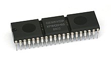
For the packaging, the Intel 8086 was available both in ceramic and plastic DIP packages.
 A ceramic D8086 variant |
 A plastic P8086 variant |
List of Intel 8086[]
| Model number | Frequency | Technology | Temperature range | Date of release | Price (USD)[list2 1] |
|---|---|---|---|---|---|
| 8086 | 5 MHz[13] | HMOS | 0 °C to 70 °C[14] | June 8, 1978[15] | $86.65[16] |
| 8086-1 | 10 MHz | HMOS II | Commercial | ||
| 8086-2 | 8 MHz[13] | HMOS II | Commercial | January/February 1980[17] | $200[17][18] |
| 8086-4 | 4 MHz[13] | HMOS | Commercial | $72.50[list2 2][19] | |
| I8086 | 5 MHz | HMOS | Industrial −40 °C to +85 °C[14] | May/June 1980[14] | $173.25[14] |
| M8086 | 5 MHz | HMOS | Military grade −55 °C to +125 °C[20] | ||
| 80C86[21] | CMOS |
Derivatives and clones[]
Compatible—and, in many cases, enhanced—versions were manufactured by Fujitsu, Harris/Intersil, OKI, Siemens, Texas Instruments, NEC, Mitsubishi, and AMD. For example, the NEC V20 and NEC V30 pair were hardware-compatible with the 8088 and 8086 even though NEC made original Intel clones μPD8088D and μPD8086D respectively, but incorporated the instruction set of the 80186 along with some (but not all) of the 80186 speed enhancements, providing a drop-in capability to upgrade both instruction set and processing speed without manufacturers having to modify their designs. Such relatively simple and low-power 8086-compatible processors in CMOS are still used in embedded systems.
The electronics industry of the Soviet Union was able to replicate the 8086 through both industrial espionage and reverse engineering[citation needed]. The resulting chip, K1810VM86, was binary and pin-compatible with the 8086.
i8086 and i8088 were respectively the cores of the Soviet-made PC-compatible and desktops. (EC1831 is the EC identification of IZOT 1036C and EC1832 is the EC identification of IZOT 1037C, developed and manufactured in Bulgaria. EC stands for Единая Система.) However, the EC1831 computer (IZOT 1036C) had significant hardware differences from the IBM PC prototype. The EC1831 was the first PC-compatible computer with dynamic bus sizing (US Pat. No 4,831,514). Later some of the EC1831 principles were adopted in PS/2 (US Pat. No 5,548,786) and some other machines (UK Patent Application, Publication No. GB-A-2211325, Published June 28, 1989).
 Soviet clone K1810VM86 |
 OKI M80C86A QFP-56 |
 NEC μPD8086D-2 (8 MHz) from the year 1984, week 19 JAPAN (clone of Intel D8086-2) |
Support chips[]
- Intel 8237: direct memory access (DMA) controller
- Intel 8251: universal synchronous/asynchronous receiver/transmitter at 19.2 kbit/s
- Intel 8253: programmable interval timer, 3x 16-bit max 10 MHz
- Intel 8255: programmable peripheral interface, 3x 8-bit I/O pins used for printer connection etc.
- Intel 8259: programmable interrupt controller
- Intel 8279: keyboard/display controller, scans a keyboard matrix and display matrix like 7-seg
- Intel 8282/8283: 8-bit latch
- Intel 8284: clock generator
- /: bidirectional 8-bit driver. In 1980 both Intel I8286/I8287 (industrial grade) version were available for US$16.25 in quantities of 100.[14]
- Intel 8288: bus controller
- Intel 8289: bus arbiter
- NEC µPD765 or Intel 8272A: floppy controller[22]
Microcomputers using the 8086[]
- The Intel Multibus-compatible single-board computer ISBC 86/12 was announced in 1978.[23]
- The Xerox NoteTaker was one of the earliest portable computer designs in 1978 and used three 8086 chips (as CPU, graphics processor, and I/O processor), but never entered commercial production.
- Seattle Computer Products shipped S-100 bus based 8086 systems (SCP200B) as early as November 1979.
- The Norwegian Mycron 2000, introduced in 1980.
- One of the most influential microcomputers of all, the IBM PC, used the Intel 8088, a version of the 8086 with an 8-bit data bus (as mentioned above).
- The first Compaq Deskpro used an 8086 running at 7.16 MHz, but was compatible with add-in cards designed for the 4.77 MHz IBM PC XT and could switch the CPU down to the lower speed (which also switched in a memory bus buffer to simulate the 8088's slower access) to avoid software timing issues.
- An 8 MHz 8086-2 was used in the AT&T 6300 PC (built by Olivetti, and known globally under several brands and model numbers), an IBM PC-compatible desktop microcomputer. The M24 / PC 6300 has IBM PC/XT compatible 8-bit expansion slots, but some of them have a proprietary extension providing the full 16-bit data bus of the 8086 CPU (similar in concept to the 16-bit slots of the IBM PC AT, but different in the design details, and physically incompatible), and all system peripherals including the onboard video system also enjoy 16-bit data transfers. The later Olivetti M24SP featured an 8086-2 running at the full maximum 10 MHz.
- The IBM PS/2 models 25 and 30 were built with an 8 MHz 8086.
- The Amstrad PC1512, PC1640, PC2086, PC3086 and PC5086 all used 8086 CPUs at 8 MHz.
- The NEC PC-9801.
- The Tandy 1000 SL-series and RL machines used 9.47 MHz 8086 CPUs.
- The IBM Displaywriter word processing machine[24] and the Wang Professional Computer, manufactured by Wang Laboratories, also used the 8086.
- NASA used original 8086 CPUs on equipment for ground-based maintenance of the Space Shuttle Discovery until the end of the space shuttle program in 2011. This decision was made to prevent software regression that might result from upgrading or from switching to imperfect clones.[25]
- KAMAN Process and Area Radiation Monitors[26]
See also[]
- Transistor count
- iAPX, for the iAPX name
Notes[]
- ^ Fewer TTL buffers, latches, multiplexers (although the amount of TTL logic was not drastically reduced). It also permits the use of cheap 8080-family ICs, where the 8254 CTC, 8255 PIO, and 8259 PIC were used in the IBM PC design. In addition, it makes PCB layout simpler and boards cheaper, as well as demanding fewer (1- or 4-bit wide) DRAM chips.
- ^ using enhancement load PMOS logic (requiring 14 V, achieving TTL compatibility by having VCC at +5 V and VDD at −9 V).
- ^ Using non-saturated enhancement-load NMOS logic (demanding a higher gate voltage for the load-transistor gates).
- ^ Made possible with depletion-load nMOS logic (the 8085 was later made using HMOS processing, just like the 8086).
- ^ Rev.0 of the instruction set and architecture was ready in about three months, according to Morse.
- ^ Using rubylith, light boards, rulers, electric erasers, and a digitizer (according to Jenny Hernandez, member of the 8086 design team, in a statement made on Intel's webpage for its 25th birthday).
- ^ 8086 used less microcode than many competitors' designs, such as the MC68000 and others
- ^ Fast static RAMs in MOS technology (as fast as bipolar RAMs) was an important product for Intel during this period.
- ^ CHMOS is Intel's name for CMOS circuits manufactured using processing steps very similar to HMOS.
- ^ Other members of the design team were Peter A.Stoll and Jenny Hernandez.
- ^ The IBM PC and PC/XT use an Intel 8088 running in maximum mode, which allows the CPU to work with an optional 8087 coprocessor installed in the math coprocessor socket on the PC or PC/XT mainboard. (The PC and PC/XT may require maximum mode for other reasons, such as perhaps to support the DMA controller.)
- ^ Some 80186 clones did change the shift value, but were never commonly used in desktop computers.
- ^ (IBM PC used 4.77 MHz, 4/3 the standard NTSC color burst frequency)
References[]
- ^ CPU History – The CPU Museum – Life Cycle of the CPU.
- ^ "Microprocessor Hall of Fame". Intel. Archived from the original on 2007-07-06. Retrieved 2007-08-11.
- ^ iAPX 286 Programmer's Reference (PDF). Intel. 1983. p. 1-1.
- ^ Jump up to: a b "Happy Birthday, 8086: Limited-Edition 8th Gen Intel Core i7-8086K Delivers Top Gaming Experience". Intel.
- ^ "8080 family". CPU World.
- ^ Scanlon, Leo J. (1988). 8086/8088/80286 assembly language. Brady Books. p. 12. ISBN 978-0-13-246919-7.
[…] The 8086 is software-compatible with the 8080 at the assembly-language level. […]
- ^ "Birth of a Standard: The Intel 8086 Microprocessor. Thirty years ago, Intel released the 8086 processor, introducing the x86 architecture that underlies every PC — Windows, Mac, or Linux — produced today". PC World. June 17, 2008.
- ^ Geiger, Randall L.; Allen, Phillip E.; Strader, Noel R. (1990). "Random Logic vs. Structured Logic Forms". VLSI design techniques for analog and digital circuits. McGraw-Hill. p. 779. ISBN 0-07-023253-9. — Illustration of use of "random" describing CPU control logic
- ^ Intel Corporation (1983). IAPX 86, 88, 186, and 188 user's manual : programmer's reference. pp. 3–5. ISBN 978-0835930352. OCLC 11091251.
- ^ Morse, Stephen P.; Ravenel, Bruce W; Mazor, Stanley; Pohlman, William B. (October 1980). "Intel Microprocessors: 8008 to 8086". IEEE Computer. 13 (10): 42–60. doi:10.1109/MC.1980.1653375. S2CID 206445851.
- ^ Jump up to: a b c Osborne, Adam; Kane, Gerry (1981). Osborne 16 bit Processor Handbook. pp. 5–26. ISBN 0-931988-43-8.
- ^ Microsoft Macro Assembler 5.0 Reference Manual. Microsoft Corporation. 1987.
Timings and encodings in this manual are used with permission of Intel and come from the following publications: Intel Corporation. iAPX 86, 88, 186 and 188 User's Manual, Programmer's Reference, Santa Clara, Calif. 1986.
(Similarly for iAPX 286, 80386, 80387.) - ^ Jump up to: a b c The 8086 Family User's Manual. Intel Corporation. October 1979. p. B-1. OCLC 65699372.
- ^ Jump up to: a b c d e Intel Corporation (May–June 1980). "8086 Available for industrial environment". Intel Preview (Special Issue: 16-Bit Solutions): 29.
- ^ "Intel® Microprocessor Quick Reference Guide - Year". www.intel.com.
- ^ Intel Corporation (May–June 1980). "The 8086 Family: Concepts and realities". Intel Preview (Special Issue: 16-Bit Solutions): 19.
- ^ Jump up to: a b Intel Corporation (January–February 1980). "New Products: Faster 8086 provides 60% more performance". Intel Preview: 22.
- ^ Intel Corporation (May–June 1980). "New 8086 family products boost processor performance by 50 percent". Intel Preview (Special Issue: 16-Bit Solutions): 17.
- ^ Intel Corporation (May–June 1979). "Microcomputer Components: New price reductions and production improvements make the popular 8086 microprocessor even more attractive". Intel Preview: 11.
- ^ Intel Corporation (August 1981). Intel iAPX86, 88 User's manual. p. B-25. ISBN 0835930165. OCLC 8459750.
- ^ Intel Corporation, "NewsBit: Intel Licenses Oki on CMOS Version of Several Products", Solutions, July/August 1984, Page 1.
- ^ "The floppy controller evolution | OS/2 Museum". 2011-05-26. Retrieved 2016-05-12.
In the original IBM PC (1981) and PC/XT (1983), the FDC was physically located on a separate diskette adapter card. The FDC itself was a NEC µPD765A or a compatible part, such as the Intel 8272A.
- ^ Enterprise, I.D.G (December 11, 1978). "Intel Adds 16-Bit Single Board". Computerworld. XII (50): 86. ISSN 0010-4841.
- ^ Zachmann, Mark (August 23, 1982). "Flaws in IBM Personal Computer frustrate critic". InfoWorld. 4 (33): 57–58. ISSN 0199-6649.
the IBM Displaywriter is noticeably more expensive than other industrial micros that use the 8086.
- ^ "For Old Parts, NASA Boldly Goes ... on eBay". New York Times. May 12, 2002.
- ^ Kaman Tech. Manual
External links[]
| Wikimedia Commons has media related to Intel 8086. |
- Intel datasheets
- List of 8086 CPUs and their clones at CPUworld.com
- 8086 Pinouts
- Maximum Mode Interface
- The 8086 User's manual October 1979 INTEL Corporation (PDF document)
- 8086 program codes using emu8086 (Version 4.08) Emulator
- Intel 8086/80186 emulator written in C, this file is part of a larger PC emulator
- Shirriff, Ken (June 2020). "A look at the die of the 8086 processor".
- — (June 2020). "Die shrink: How Intel scaled down the 8086 processor".
- — (July 2020). "The Intel 8086 processor's registers: from chip to transistors".
- — (August 2020). "Reverse-engineering the adder inside the Intel 8086".
- — (August 2020). "Reverse-engineering the 8086's Arithmetic/Logic Unit from die photos".
| show Authority control |
|---|
- Intel microprocessors
- Computer-related introductions in 1978
- Intel x86 microprocessors
- 16-bit microprocessors