Skylake (microarchitecture)
It has been suggested that this article be split into articles titled and Skylake (microarchitecture). (Discuss) (April 2021) |
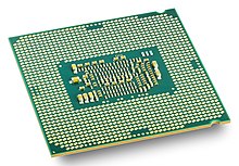 Intel Core i7-6700K with four physical cores | |
| General information | |
|---|---|
| Launched | August 5, 2015 |
| Discontinued | March 4, 2019 (desktop processors) |
| Marketed by | Intel |
| Designed by | Intel |
| Common manufacturer(s) |
|
| CPUID code | 0406e3h, 0506e3h |
| Product code |
|
| Performance | |
| Max. CPU clock rate | Up to 4.5 GHz |
| Cache | |
| L1 cache | 64 KB per core |
| L2 cache | 256 KB per core (1 MB per core for Skylake-X) |
| L3 cache | Up to 2 MB per core (1.375 MB per core for Skylake-X) |
| L4 cache | 128 MB of eDRAM (on some models) |
| Architecture and classification | |
| Technology node | 14 nm bulk silicon 3D transistors (Tri-Gate) |
| Architecture | x86-64 |
| Microarchitecture | Skylake |
| Instruction set | x86-64 |
| Instructions | x86-64 (Intel 64) |
| Extensions | |
| Physical specifications | |
| Cores |
|
| Socket(s) | |
| Products, models, variants | |
| Brand name(s) |
|
| History | |
| Predecessor | Broadwell (Tick/Process) |
| Successor |
|
Skylake[6][7] is the codename used by Intel for a processor microarchitecture that was launched in August 2015[8] succeeding the Broadwell microarchitecture.[9] Skylake is a microarchitecture redesign using the same 14 nm manufacturing process technology[10] as its predecessor, serving as a tock in Intel's tick–tock manufacturing and design model. According to Intel, the redesign brings greater CPU and GPU performance and reduced power consumption. Skylake CPUs share their microarchitecture with Kaby Lake, Coffee Lake, Cannon Lake, Whiskey Lake, and Comet Lake CPUs.
Skylake is the last Intel platform on which Windows earlier than Windows 10 will be officially supported by Microsoft,[11] although enthusiast-created modifications exist that allow Windows 8.1 and earlier to continue to receive Windows Updates on later platforms.[12][13][14]
Some of the processors based on the Skylake microarchitecture are marketed as 6th-generation Core.[15][16][17]
Intel officially declared end of life and discontinued Skylake LGA 1151 CPUs on March 4, 2019.[18]
Development history[]
Skylake's development, as with previous processors such as Banias, Dothan, Conroe, Sandy Bridge, and Ivy Bridge, was primarily undertaken by Intel Israel at its engineering research center in Haifa, Israel.[19] The final design was largely an evolution of Haswell, with minor improvements to performance and several power-saving features being added.[20] A major priority of Skylake's design was to design a microarchitecture for envelopes as low as 4.5W to embed within tablet computers and notebooks in addition to higher-power desktop computers and servers.[21]
In September 2014, Intel announced the Skylake microarchitecture at the Intel Developer Forum in San Francisco, and that volume shipments of Skylake CPUs were scheduled for the second half of 2015. The Skylake development platform was announced to be available in Q1 2015. During the announcement, Intel also demonstrated two computers with desktop and mobile Skylake prototypes: the first was a desktop testbed system, running the latest version of 3DMark, while the second computer was a fully functional laptop, playing 4K video.[22]
An initial batch of Skylake CPU models (6600K and 6700K) was announced for immediate availability during the Gamescom on August 5, 2015,[23] unusually soon after the release of its predecessor, Broadwell, which had suffered from launch delays.[24] Intel acknowledged in 2014 that moving from 22 nm (Haswell) to 14 nm (Broadwell) had been its most difficult process to develop yet, causing Broadwell's planned launch to slip by several months;[25] yet, the 14 nm production was back on track and in full production as of Q3 2014.[26] Industry observers had initially believed that the issues affecting Broadwell would also cause Skylake to slip to 2016, but Intel was able to bring forward Skylake's release and shorten Broadwell's release cycle instead.[27][28] As a result, the Broadwell architecture had an unusually short run.[27]
Overclocking of unsupported processors[]
Officially Intel supported overclocking of only the K and X versions of Skylake processors. However, it was later discovered that other non-K chips could be overclocked by modifying the base clock value – a process made feasible by the base clock applying only to the CPU, RAM, and integrated graphics on Skylake. Through beta UEFI firmware updates, some motherboard vendors, such as ASRock (which prominently promoted it under the name Sky OC) allowed the base clock to be modified in this manner.[29][30]
When overclocking unsupported processors using these UEFI firmware updates, several issues arise:
- C-states are disabled, therefore the CPU will constantly run at its highest frequency and voltage
- Turbo-boost is disabled
- Integrated graphics are disabled
- AVX2 instruction performance is poor, approximately 4-5 times slower due to the upper 128-bit half of the execution units and data buses not being taken out of their power saving states
- CPU core temperature readings are incorrect
These issues are partly caused by the power management of the processor needing to be disabled for base clock overclocking to work.[31]
In February 2016, however, an ASRock firmware update removed the feature. On February 9, 2016, Intel announced that it would no longer allow such overclocking of non-K processors, and that it had issued a CPU microcode update that removes the function.[32][33][34] In April 2016, ASRock started selling motherboards that allow overclocking of unsupported CPUs using an external clock generator.[35][36]
Operating system support[]
In January 2016, Microsoft announced that it would end support of Windows 7 and Windows 8.1 on Skylake processors effective July 17, 2017; after this date, only the most critical updates for the two operating systems would be released for Skylake users if they have been judged not to affect the reliability of the OS on older hardware, and Windows 10 would be the only Microsoft Windows platform officially supported on Skylake, as well as all future Intel CPU microarchitectures beginning with Skylake's successor Kaby Lake. Terry Myerson stated that Microsoft had to make a large investment in order to reliably support Skylake on older versions of Windows, and that future generations of processors would require further investments. Microsoft also stated that due to the age of the platform, it would be challenging for newer hardware, firmware, and device driver combinations to properly run under Windows 7.[37][38]
On March 18, 2016, in response to criticism over the move, primarily from enterprise customers, Microsoft announced revisions to the support policy, changing the cutoff for support and non-critical updates to July 17, 2018 and stating that Skylake users would receive all critical security updates for Windows 7 and 8.1 through the end of extended support.[39][40] In August 2016, citing a strong partnership with our OEM partners and Intel, Microsoft stated that it would continue to fully support 7 and 8.1 on Skylake through the end of their respective lifecycles.[41][42] In addition, an enthusiast-created modification was released that disabled the Windows Update check and allowed Windows 8.1 and earlier to continue to be updated on this and later platforms.[43]
As of Linux kernel 4.10, Skylake mobile power management is supported with most Package C states supported seeing some use. Linux 4.11 enables Frame-Buffer Compression for the integrated graphics chipset by default, which lowers power consumption.[44]
Skylake is fully supported on OpenBSD 6.2 and later, including accelerated graphics.[45]
For Windows 11, only the high-end Skylake-X processors are officially listed as compatible.[46] All other Skylake processors are not officially supported due to security concerns.[47] However, it is still possible to manually upgrade using an ISO image (as Windows 10 users on those processors won't be offered to upgrade to Windows 11 via Windows Update), or perform a clean installation as long as the system has Trusted Platform Module (TPM) 2.0 enabled,[48] but the user must accept that they will not be entitled to receive updates, and that damage caused by using Windows 11 on an unsupported configuration are not covered by the manufacturer's warranty.[49][50]
Features[]

Like its predecessor, Broadwell, Skylake is available in five variants, identified by the suffixes S (SKL-S), X (SKL-X), H (SKL-H), U (SKL-U), and Y (SKL-Y). SKL-S and SKL-X contain overclockable K and X variants with unlocked multipliers.[51] The H, U and Y variants are manufactured in ball grid array (BGA) packaging, while the S and X variants are manufactured in land grid array (LGA) packaging using a new socket, LGA 1151 (LGA 2066 for Skylake X).[52] Skylake is used in conjunction with Intel 100 Series chipsets, also known as Sunrise Point.[53]
The major changes between the Haswell and Skylake architectures include the removal of the fully integrated voltage regulator (FIVR) introduced with Haswell.[54] On the variants that will use a discrete Platform Controller Hub (PCH), Direct Media Interface (DMI) 2.0 is replaced by DMI 3.0, which allows speeds of up to 8 GT/s.
Skylake's U and Y variants support one DIMM slot per channel, while H and S variants support two DIMM slots per channel.[52] Skylake's launch and sales lifespan occur at the same time as the ongoing SDRAM market transition, with DDR3 SDRAM memory gradually being replaced by DDR4 memory. Rather than working exclusively with DDR4, the Skylake microarchitecture remains backward compatible by interoperating with both types of memory. Accompanying the microarchitecture's support for both memory standards, a new SO-DIMM type capable of carrying either DDR3 or DDR4 memory chips, called UniDIMM, was also announced.[55]
Skylake's few P variants have a reduced on-die graphics unit (12 execution units enabled instead of 24 execution units) over their direct counterparts; see the table below. In contrast, with Ivy Bridge CPUs the P suffix was used for CPUs with completely disabled on-die video chipset.
Other enhancements include Thunderbolt 3.0, SATA Express, Iris Pro graphics with Direct3D feature level 12_1 with up to 128 MB of L4 eDRAM cache on certain SKUs.[56] The Skylake line of processors retires VGA support,[57] while supporting up to five monitors connected via HDMI 1.4, DisplayPort 1.2 or Embedded DisplayPort (eDP) interfaces.[58] HDMI 2.0 (4K@60 Hz) is only supported on motherboards equipped with Intel's Alpine Ridge Thunderbolt controller.[59]
The Skylake instruction set changes include Intel MPX (Memory Protection Extensions) and Intel SGX (Software Guard Extensions). Future Xeon variants will also have Advanced Vector Extensions 3.2 (AVX-512F).[3][4]
Skylake-based laptops were predicted to use wireless technology called Rezence for charging, and other wireless technologies for communication with peripherals. Many major PC vendors agreed to use this technology in Skylake-based laptops; however, no laptops were released with the technology as of 2019.[60][61]
The integrated GPU of Skylake's S variant supports on Windows DirectX 12 Feature Level 12_1, OpenGL 4.6 with latest Windows 10 driver update[62] (OpenGL 4.5 on Linux[63]) and OpenCL 3.0 standards, as well as some modern hardware video encoding/decoding formats such as VP9 (GPU accelerated decode only), VP8 and HEVC (hardware accelerated 8-bit encode/decode and GPU accelerated 10-bit decode).[64][65]
Intel also released unlocked (capable of overclocking) mobile Skylake CPUs.[66]
Unlike previous generations, Skylake-based Xeon E3 no longer works with a desktop chipset that supports the same socket, and requires either the C232 or the C236 chipset to operate.
Known issues[]
Short loops with a specific combination of instruction use may cause unpredictable system behavior on CPUs with hyperthreading. A microcode update was issued to fix the issue.[67]
Skylake is vulnerable to Spectre attacks.[68] In fact, it is more vulnerable than other processors because it uses indirect branch speculation not just on indirect branches but also when the return prediction stack underflows.
The latency for the spinlock PAUSE instruction has been increased dramatically (from the usual 10 cycles to 141 cycles in Skylake), which can cause performance issues with older programs or libraries using pause instructions.[69] Intel documents the increased latency as a feature that improves power efficiency.[70]
Architecture changes compared to Broadwell microarchitecture[]
CPU[]
- Improved front-end, deeper out-of-order buffers, improved execution units, more execution units (third vector integer ALU(VALU)) for five ALUs in total, more load/store bandwidth, improved hyper-threading (wider retirement), speedup of AES-GCM and AES-CBC by 17% and 33% accordingly.[71][72]
- Up to four cores as the default mainstream configuration[73] and up to 18 cores for X-series
- AVX-512: F, CD, VL, BW, and DQ for some future Xeon variants, but not Xeon E3[3]
- Intel MPX (Memory Protection Extensions)
- Intel SGX (Software Guard Extensions)
- Intel Speed Shift[74]
- Larger Re-order buffer (224 entries, up from 192)
- L1 cache size unchanged at 32 KB instruction and 32 KB data cache per core.
- L2 cache was changed from 8-way to 4-way set associative[75]
- Voltage regulator module (FIVR) is moved back to the motherboard
- Enhancements of Intel Processor Trace: fine grained timing through CYC packets (cycle-accurate mode) and support for IP (Instruction Pointer) address filtering.[76]
- 64 to 128 MB L4 eDRAM cache on certain SKUs
GPU[]
- Skylake's integrated Gen9 GPU supports Direct3D 12 at the feature level 12_1[6][77][78]
- Full fixed function HEVC Main/8bit encoding/decoding acceleration. Hybrid/Partial HEVC Main10/10bit decoding acceleration. JPEG encoding acceleration for resolutions up to 16,000×16,000 pixels. Partial VP9 encoding/decoding acceleration.[79]
I/O[]
- LGA 1151 socket for mainstream desktop processors and LGA 2066 socket for enthusiast gaming/workstation X-series processors
- 100-series chipset (Sunrise Point)[80]
- X-series uses X299-series chipset
- DMI 3.0 (From DMI 2.0)
- Support for both DDR3L SDRAM and DDR4 SDRAM in mainstream variants, using custom UniDIMM SO-DIMM form factor[73][81][82] with up to 64 GB of RAM on LGA 1151 variants. Usual DDR3 memory is also supported by certain motherboard vendors even though Intel doesn't officially support it.[83][84]
- Support for 16 PCI Express 3.0 lanes from CPU, 20 PCI Express 3.0 lanes from PCH (LGA 1151), 44 PCI Express 3.0 lanes for Skylake-X
- Support for Thunderbolt 3 (Alpine Ridge)[85]
Other[]
- Thermal design power (TDP) up to 95 W (LGA 1151); up to 165 W (LGA 2066)[86]
- 14 nm manufacturing process[87]
Configurations[]
Skylake processors are produced in five main families: Y, U, H, S, and X. Multiple configurations are available within each family:[52]
| Feature | Family | ||||||||
|---|---|---|---|---|---|---|---|---|---|
| Y | U | H | T | S | R | X | W | SP | |
| Integrated L4 cache | • | • | • | ||||||
| Low-power mobile/embedded systems | • | • | • | • | |||||
| Socket | BGA | LGA 1151 | LGA 2066 | LGA 3647 | |||||
| DDR3L SDRAM | • | • | • | • | • | • | |||
| DDR4 SDRAM | • | • | • | • | • | • | • | ||
| 128 GB (GB) of physical RAM | • | • | •+ | ||||||
| 28 to 44 PCIe 3.0 lanes |
• | • | • | ||||||
List of Skylake processor models[]
Mainstream desktop processors[]

Common features of the mainstream desktop Skylake CPUs:
- DMI 3.0 and PCIe 3.0 interfaces
- Dual channel memory support in the following configurations: DDR3L-1600 1.35 V (32 GB maximum) or DDR4-2133 1.2 V (64 GB maximum). DDR3 is unofficially supported through some motherboard vendors[88][89][90]
- 16 PCI-E 3.0 lanes
- The Core-branded processors support the AVX2 instruction set. The Celeron and Pentium-branded ones support only SSE4.1/4.2
- 350 MHz base graphics clock rate
| Cores (threads) |
Processor branding and model |
CPU clock rate |
Turbo clock GHz
Num of cores |
GPU | EUs | Max graphics clock rate |
L2 cache |
L3 cache |
L4 cache (eDRAM) |
TDP | Socket | Release date |
Release price (USD) | |||
|---|---|---|---|---|---|---|---|---|---|---|---|---|---|---|---|---|
| 1 | 2 | 4 | ||||||||||||||
| 4 (8) | Core i7 | 6700K | 4.0 GHz | 4.2 | 4.0 | 4.0 | HD 530 | 24 | 1150 MHz [91] | 4 ×
256 KB |
8 MB | N/A | 91 W | LGA 1151 | August 5, 2015 | $339 |
| 6785R | 3.3 GHz | 3.9 | 3.8 | 3.5 | Iris Pro 580 | 72 | 128 MB | 65 W | FCBGA1440 | May 3, 2016 | $370 | |||||
| 6700 | 3.4 GHz | 4.0 | 3.9 | 3.7 | HD 530 | 24 | N/A | LGA 1151 | September 1, 2015 | $303 | ||||||
| 6700T | 2.8 GHz | 3.6 | 3.5 | 3.4 | 35 W | $303 | ||||||||||
| 4 (4) | Core i5 | 6600K | 3.5 GHz | 3.9 | 3.8 | 3.6 | 6 MB | 91 W | August 5, 2015 | $242 | ||||||
| 6685R | 3.2 GHz | 3.8 | 3.7 | 3.3 | Iris Pro 580 | 72 | 128 MB | 65 W | FCBGA1440 | May 3, 2016 | $288 | |||||
| 6600 | 3.3 GHz | 3.9 | 3.8 | 3.6 | HD 530 | 24 | N/A | LGA 1151 | September 1, 2015 | $213 | ||||||
| 6585R | 2.8 GHz | 3.6 | 3.5 | 3.1 | Iris Pro 580 | 72 | 1100 MHz | 128 MB | FCBGA1440 | May 3, 2016 | $255 | |||||
| 6500 | 3.2 GHz | 3.3 | HD 530 | 24 | 1050 MHz | N/A | LGA 1151 | September 1, 2015 | $192 | |||||||
| 6600T | 2.7 GHz | 3.5 | 3.4 | 3.3 | 1100 MHz | 35 W | Q3 2015 | $213 | ||||||||
| 6500T | 2.5 GHz | 3.1 | 3.0 | 2.8 | $192 | |||||||||||
| 6402P | 2.8 GHz | 3.4 | 3.4 | 3.2 | HD 510 | 12 | 950 MHz | 65 W | December 27, 2015 | $182 | ||||||
| 6400T | 2.2 GHz | 2.8 | 2.7 | 2.5 | HD 530 | 24 | 35 W | Q3 2015 | ||||||||
| 6400 | 2.7 GHz | 3.3 | 3.3 | 3.1 | 65 W | August 5, 2015 | ||||||||||
| 2 (4) | Core i3 | 6320 | 3.9 GHz | N/A | 1150 MHz | 2 ×
256 KB |
4 MB | 51 W | Q3 2015 | $149 | ||||||
| 6300 | 3.8 GHz | $138 | ||||||||||||||
| 6100 | 3.7 GHz | 1050 MHz | 3 MB | October 2015 | $117 | |||||||||||
| 6300T | 3.3 GHz | 950 MHz | 4 MB | 35 W | $138 | |||||||||||
| 6100T | 3.2 GHz | 3 MB | $117 | |||||||||||||
| 6098P | 3.6 GHz | HD 510 | 12 | 1050 MHz | 54 W | December 27, 2015 | ||||||||||
| 2 (2) | Pentium | G4520 | 3.6 GHz | HD 530 | 24 | 51 W | October 2015 | $86 | ||||||||
| G4500 | 3.5 GHz | $75 | ||||||||||||||
| G4500T | 3.0 GHz | 950 MHz | 35 W | Q3 2015 | ||||||||||||
| G4400 | 3.3 GHz | HD 510 | 12 | 1000 MHz | 54 W | October 2015 | $64 | |||||||||
| G4400T | 2.9 GHz | 950 MHz | 35 W | Q3 2015 | ||||||||||||
| G4400TE | 2.4 GHz | Q4 2015 | $70 | |||||||||||||
| Celeron | G3920 | 2.9 GHz | 2 MB | 51 W | $52 | |||||||||||
| G3900 | 2.8 GHz | $42 | ||||||||||||||
| G3900TE | 2.3 GHz | 35 W | ||||||||||||||
| G3900T | 2.6 GHz | |||||||||||||||
High-end desktop processors (Skylake-X)[]
Common features of the high performance Skylake-X CPUs:
- Quad channel memory support for DDR4-2400 (on the i7-7800X) or DDR4-2666 (on all other CPUs)[92] up to 128 GB
- 28 (for the i7-7800X and i7-7820X) to 44 (for all other CPUs) PCI-E 3.0 lanes
- In addition to the AVX2 instruction set, they also support the AVX-512 instructions
- No built-in iGPU (integrated graphics processor)
- Turbo Boost Max Technology 3.0 for up to 2/4 threads workloads for CPUs that have 8 cores and more (7820X, 7900X, 7920X, 7940X, 7960X, 7980XE, and all 9th generation chips)[93]
- A different cache hierarchy (when compared to client Skylake CPUs or previous architectures)

| Cores (threads) |
Processor branding and model |
CPU clock rate |
Turbo clock GHz | L2 cache |
L3 cache |
TDP | Socket | Release date |
Release price (USD) | ||
|---|---|---|---|---|---|---|---|---|---|---|---|
| TB 2.0 | TB Max 3.0 | ||||||||||
| 18 (36) | Core i9 [94] | 7980XE | 2.6 GHz | 4.2 | 4.4 | 1 MB per core |
1⅜ MB per core |
165 W | LGA 2066 | September 25, 2017[95] |
$1999 |
| 16 (32) | 7960X | 2.8 GHz | $1699 | ||||||||
| 14 (28) | 7940X | 3.1 GHz | 4.3 | $1399 | |||||||
| 12 (24) | 7920X | 2.9 GHz | 140 W | August 28, 2017 | $1189 | ||||||
| 10 (20) | 7900X | 3.3 GHz | 4.5 | June 19, 2017 | $999 | ||||||
| 8 (16) | Core i7 | 7820X | 3.6 GHz | $599 | |||||||
| 6 (12) | 7800X | 3.5 GHz | 4.0 | N/A | $389 | ||||||
| Cores (threads) |
Processor branding and model |
CPU clock rate |
Turbo clock GHz | L2 cache |
L3 cache |
TDP | Socket | Release date |
Release price (USD) | ||
|---|---|---|---|---|---|---|---|---|---|---|---|
| TB 2.0 | TB Max 3.0 | ||||||||||
| 14 (28) | Core i9 [96] | 9990XE[97] | 4.0 GHz | 5.0 | 5.0 | 1 MB per core |
19.25 MB | 255 W | LGA 2066 | January 3, 2019 | OEM only |
| 18 (36) | 9980XE | 3.0 GHz | 4.4 | 4.5 | 24.75 MB | 165 W | October 9, 2018[98] | $1979 | |||
| 16 (32) | 9960X | 3.1 GHz | 22 MB | $1684 | |||||||
| 14 (28) | 9940X | 3.3 GHz | 19.25 MB | $1387 | |||||||
| 12 (24) | 9920X | 3.5 GHz | $1189 | ||||||||
| 10 (20) | 9900X | 3.5 GHz | $989 | ||||||||
| 9820X | 3.3 GHz | 4.1 | 4.2 | 16.5 MB | $889 | ||||||
| 8 (16) | Core i7 | 9800X | 3.8 GHz[99] | 4.4 | 4.5 | $589 | |||||
Xeon High-end desktop processors (Skylake-X)[]
- Is Xeon instead of Core
- Uses C621 Chipset
- Xeon W-3175X is the only Xeon with a multiplier unlocked for overclocking
| Model number |
sSpec number |
Cores (threads) |
Frequency | Turbo Boost all-core/2.0 (/max. 3.0) |
L2 cache |
L3 cache |
TDP | Socket | I/O bus | Memory | Release date | Part number(s) |
Release price (USD) |
|---|---|---|---|---|---|---|---|---|---|---|---|---|---|
| Xeon W-3175X |
|
28 (56) | 3.1 GHz | 3.8/4.3 GHz | 28 × 1 MB | 38.50 MB | 255 W
|
LGA 3647 | DMI 3.0 | 6 × DDR4-2666 | January 30, 2019 |
|
$2999 |
Mobile processors[]
See also Server, Mobile below for mobile workstation processors.
| Target segment |
Cores (threads) |
Processor branding and model |
CPU clock rate |
CPU Turbo clock rate | GPU | GPU clock rate | L3 cache |
L4 cache |
Max. PCIe lanes |
TDP | cTDP | Release date | Price (USD) | |||||
|---|---|---|---|---|---|---|---|---|---|---|---|---|---|---|---|---|---|---|
| Single core |
Dual core |
Quad core |
Base | Max | Up | Down | ||||||||||||
| Performance | 4 (8) | Core i7 | 6970HQ | 2.8 GHz | 3.7 GHz | ? | Iris Pro 580 | 350 MHz | 1050 MHz | 8 MB | 128 MB | 16 | 45 W | N/A | 35 W | Q1 2016 | $623 | |
| 6920HQ | 2.9 GHz | 3.8 GHz | 3.6 GHz | 3.4 GHz | HD 530 | N/A | September 1, 2015 | $568 | ||||||||||
| 6870HQ | 2.7 GHz | 3.6 GHz | ? | Iris Pro 580 | 1000 MHz | 128 MB | Q1 2016 | $434 | ||||||||||
| 6820HQ | 3.4 GHz | 3.2 GHz | HD 530 | 1050 MHz | N/A | September 1, 2015 | $378 | |||||||||||
| 6820HK | ||||||||||||||||||
| 6770HQ | 2.6 GHz | 3.5 GHz | ? | Iris Pro 580 | 950 MHz | 6 MB | 128 MB | Q1 2016 | $434 | |||||||||
| 6700HQ | 3.3 GHz | 3.1 GHz | HD 530 | 1050 MHz | N/A | September 1, 2015 | $378 | |||||||||||
| Mainstream | 2 (4) | 6660U | 2.4 GHz | 3.4 GHz | 3.2 GHz | N/A | Iris 540 | 300 MHz | 4 MB | 64 MB | 12 | 15 W | 9.5 W | Q1 2016 | $415 | |||
| 6650U | 2.2 GHz | Q3 2015 | ||||||||||||||||
| 6600U | 2.6 GHz | N/A | HD 520 | N/A | 25 W | 7.5 W | September 1, 2015 | $393 | ||||||||||
| 6567U | 3.3 GHz | 3.6 GHz | 3.4 GHz | Iris 550 | 1100 MHz | 64 MB | 28 W | N/A | 23 W | Q3 2015 | TBD | |||||||
| 6560U | 2.2 GHz | 3.2 GHz | 3.1 GHz | Iris 540 | 1050 MHz | 15 W | 9.5 W | |||||||||||
| 6500U | 2.5 GHz | 3.1 GHz | 3.0 GHz | HD 520 | N/A | 7.5 W | September 1, 2015 | $393 | ||||||||||
| 4 (4) | Core i5 | 6440HQ | 2.6 GHz | 3.5 GHz | 3.3 GHz | 3.1 GHz | HD 530 | 350 MHz | 950 MHz | 6 MB | 16 | 45 W | 35 W | $250 | ||||
| 2 (4) | 6360U | 2.0 GHz | 3.1 GHz | 2.9 GHz | N/A | Iris 540 | 300 MHz | 1000 MHz | 4 MB | 64 MB | 12 | 15 W | 9.5 W | Q3 2015 | $304 | |||
| 4 (4) | 6350HQ | 2.3 GHz | 3.2 GHz | ? | Iris Pro 580 | 350 MHz | 900 MHz | 6 MB | 128 MB | 16 | 45 W | 35 W | Q1 2016 | $306 | ||||
| 6300HQ | 3.0 GHz | 2.8 GHz | HD 530 | 950 MHz | N/A | September 1, 2015 | $250 | |||||||||||
| 2 (4) | 6300U | 2.4 GHz | 3.0 GHz | 2.9 GHz | N/A | HD 520 | 300 MHz | 1000 MHz | 3 MB | 12 | 15 W | 7.5 W | $281 | |||||
| 6287U | 3.1 GHz | 3.5 GHz | 3.3 GHz | Iris 550 | 1100 MHz | 4 MB | 64 MB | 28 W | 23 W | Q3 2015 | $304 | |||||||
| 6267U | 2.9 GHz | 3.3 GHz | 3.1 GHz | 1050 MHz | 23 W | |||||||||||||
| 6260U | 1.8 GHz | 2.9 GHz | 2.7 GHz | Iris 540 | 950 MHz | 15 W | 9.5 W | $304 | ||||||||||
| 6200U | 2.3 GHz | 2.8 GHz | HD 520 | 1000 MHz | 3 MB | N/A | 7.5 W | September 1, 2015 | $281 | |||||||||
| Core i3 | 6167U | 2.7 GHz | N/A | N/A | Iris 550 | 64 MB | 28 W | 23 W | Q3 2015 | $304 | ||||||||
| 6157U | 2.4 GHz | Q3 2016 | ||||||||||||||||
| 6100H | 2.7 GHz | HD 530 | 350 MHz | 900 MHz | N/A | 35 W | N/A | September 1, 2015 | $225 | |||||||||
| 6100U | 2.3 GHz | HD 520 | 300 MHz | 1000 MHz | 15 W | 7.5 W | $281 | |||||||||||
| 6006U | 2.0 GHz | 900 MHz | N/A | November, 2016 | $281 | |||||||||||||
| Core m7 | 6Y75 | 1.2 GHz | 3.1 GHz | 2.9 GHz | HD 515 | 300 MHz | 1000 MHz | 4 MB | 10 | 4.5 W | 7 W | 3.5 W | September 1, 2015 | $393 | ||||
| Core m5 | 6Y57 | 1.1 GHz | 2.8 GHz | 2.4 GHz | 900 MHz | $281 | ||||||||||||
| 6Y54 | 2.7 GHz | |||||||||||||||||
| Core m3 | 6Y30 | 0.9 GHz | 2.2 GHz | 2.0 GHz | 850 MHz | 3.8 W | ||||||||||||
| Pentium | 4405U | 2.1 GHz | N/A | N/A | HD 510 | 950 MHz | 2 MB | 15 W | N/A | 10 W | Q3 2015 | $161 | ||||||
| 4405Y | 1.5 GHz | HD 515 | 800 MHz | 6 W | 4.5 W | |||||||||||||
| 2 (2) | Celeron | G3902E | 1.6 GHz | N/A | HD 510 | 350 MHz | 950 MHz | 16 | 25 W | N/A | Q1 2016 | $107 | ||||||
| G3900E | 2.4 GHz | 35 W | ||||||||||||||||
| 3955U | 2.0 GHz | 300 MHz | 900 MHz | 10 | 15 W | 10 W | Q4 2015 | |||||||||||
| 3855U | 1.6 GHz | |||||||||||||||||
Workstation processors[]
- All models support: MMX, SSE, SSE2, SSE3, SSSE3, SSE4.1, SSE4.2, AVX, AVX2, AVX-512, FMA3, MPX, Enhanced Intel SpeedStep Technology (EIST), Intel 64, XD bit (an NX bit implementation), Intel VT-x, Intel VT-d, Turbo Boost (excluding W-2102 and W-2104), Hyper-threading (excluding W-2102 and W-2104), AES-NI, Intel TSX-NI, Smart Cache.
- PCI Express lanes: 48
- Supports up to 8 DIMMs of DDR4 memory, maximum 512 GB.
| Model number |
sSpec number |
Cores (threads) |
Frequency | Turbo Boost all-core/2.0 (/max. 3.0) |
L2 cache |
L3 cache |
TDP | Socket | I/O bus | Memory | Release date | Part number(s) |
Release price (USD) |
|---|---|---|---|---|---|---|---|---|---|---|---|---|---|
| Xeon W-2102 |
|
4 (4) | 2.9 GHz | N/A | 4 × 1 MB | 8.25 MB | 120 W
|
LGA 2066 | DMI 3.0 | 4 × DDR4-2400 | August 29, 2017 |
|
$202 |
| Xeon W-2104 |
|
4 (4) | 3.2 GHz | N/A | 4 × 1 MB | 8.25 MB | 120 W
|
LGA 2066 | DMI 3.0 | 4 × DDR4-2400 | August 29, 2017 |
|
$255 |
| Xeon W-2123 |
|
4 (8) | 3.6 GHz | /3.9 GHz | 4 × 1 MB | 8.25 MB | 120 W
|
LGA 2066 | DMI 3.0 | 4 × DDR4-2666 | August 29, 2017 |
|
$294 |
| Xeon W-2125 |
|
4 (8) | 4 GHz | /4.5 GHz | 4 × 1 MB | 8.25 MB | 120 W
|
LGA 2066 | DMI 3.0 | 4 × DDR4-2666 | August 29, 2017 |
|
$444 |
| Xeon W-2133 |
|
6 (12) | 3.6 GHz | /3.9 GHz | 6 × 1 MB | 8.25 MB | 140 W
|
LGA 2066 | DMI 3.0 | 4 × DDR4-2666 | August 29, 2017 |
|
$617 |
| Xeon W-2135 |
|
6 (12) | 3.7 GHz | /4.5 GHz | 6 × 1 MB | 8.25 MB | 140 W
|
LGA 2066 | DMI 3.0 | 4 × DDR4-2666 | August 29, 2017 |
|
$835 |
| Xeon W-2140B | 8 (16) | 3.2 GHz | /4.2 GHz | 8 × 1 MB | 11.00 MB | LGA 2066 | DMI 3.0 | 4 × DDR4-2666 | December 21, 2017 | OEM for Apple[100][101] | |||
| Xeon W-2145 |
|
8 (16) | 3.7 GHz | /4.5 GHz | 8 × 1 MB | 11.00 MB | 140 W
|
LGA 2066 | DMI 3.0 | 4 × DDR4-2666 | August 29, 2017 |
|
$1113 |
| Xeon W-2150B | 10 (20) | 3 GHz | /4.5 GHz | 10 × 1 MB | 13.75 MB | LGA 2066 | DMI 3.0 | 4 × DDR4-2666 | December 21, 2017 | OEM for Apple[100][101] | |||
| Xeon W-2155 |
|
10 (20) | 3.3 GHz | /4.5 GHz | 10 × 1 MB | 13.75 MB | 140 W
|
LGA 2066 | DMI 3.0 | 4 × DDR4-2666 | August 29, 2017 |
|
$1440 |
| Xeon W-2170B | 14 (28) | 2.5 GHz | /4.3 GHz | 14 × 1 MB | 19.25 MB | LGA 2066 | DMI 3.0 | 4 × DDR4-2666 | December 21, 2018 | OEM for Apple[100][101] | |||
| Xeon W-2175 |
|
14 (28) | 2.5 GHz | /4.3 GHz | 14 × 1 MB | 19.25 MB | 140 W
|
LGA 2066 | DMI 3.0 | 4 × DDR4-2666 | October 15, 2017 |
|
$1947 |
| Xeon W-2191B | 18 (36) | 2.3 GHz | /4.3 GHz | 18 × 1 MB | 24.75 MB | LGA 2066 | DMI 3.0 | 4 × DDR4-2666 | December 21, 2017 | OEM for Apple[100][101] | |||
| Xeon W-2195 |
|
18 (36) | 2.3 GHz | /4.3 GHz | 18 × 1 MB | 24.75 MB | 140 W
|
LGA 2066 | DMI 3.0 | 4 × DDR4-2666 | August 29, 2017 |
|
$2553 |
Server processors[]
E3 series server chips all consist of System Bus 9 GT/s, max. memory bandwidth of 34.1 GB/s dual channel memory. Unlike its predecessor, the Skylake Xeon CPUs require C230 series (C232/C236) or C240 series (C242/C246) chipset to operate, with integrated graphics working only with C236 and C246 chipsets. Mobile counterparts uses CM230 and CM240 series chipsets.
| Target segment |
Cores (threads) |
Processor branding and model |
GPU | Clock rate | L3 cache |
L4 cache |
TDP | Release date |
Release price (USD) tray / box |
Motherboard | ||||||
|---|---|---|---|---|---|---|---|---|---|---|---|---|---|---|---|---|
| CPU | Graphics | Socket | Interface | Memory | ||||||||||||
| Normal | Turbo | Normal | Turbo | |||||||||||||
| Server | 4 (8) | Xeon E3 v5 | 1280v5 | N/A | 3.7 GHz | 4.0 GHz | N/A | 8 MB | N/A | 80 W | Q4 15 | $612 / — | LGA 1151 |
DMI 3 PCIe 3.0 |
DDR4 2133/1866 or DDR3L 1333/1600 with ECC | |
| 1275v5 | HD P530 | 3.6 GHz | 350 MHz | 1.15 GHz | $339 / — | |||||||||||
| 1270v5 | N/A | 3.6 GHz | N/A | $328 / $339 | ||||||||||||
| 1260Lv5 | 2.9 GHz | 3.9 GHz | 45 W | $294 / — | ||||||||||||
| 1245v5 | HD P530 | 3.5 GHz | 350 MHz | 1.15 GHz | 80 W | $284 / — | ||||||||||
| 1240v5 | N/A | 3.5 GHz | N/A | $272 / $282 | ||||||||||||
| 1240Lv5 | 2.1 GHz | 3.2 GHz | 25 W | $278 / — | ||||||||||||
| 1230v5 | 3.4 GHz | 3.8 GHz | 80 W | $250 / $260 | ||||||||||||
| 4 (4) | 1235Lv5 | HD P530 | 2.0 GHz | 3.0 GHz | 350 MHz | 1.15 GHz | 25 W | $250 / — | ||||||||
| 1225v5 | 3.3 GHz | 3.7 GHz | 80 W | $213 / — | ||||||||||||
| 1220v5 | N/A | 3.0 GHz | 3.5 GHz | N/A | $193 / — | |||||||||||
| Mobile | 4 (8) | 1575Mv5 | Iris Pro 580 | 3.0 GHz | 3.9 GHz | 350 MHz | 1.1 GHz | 128 MB | 45 W | Q1 16 | $1207 / — | DDR4-2133 LPDDR3-1866 DDR3L-1600 with ECC | ||||
| 1545Mv5 | 2.9 GHz | 3.8 GHz | 1.05 GHz | $679 / — | ||||||||||||
| 1535Mv5 | HD P530 | N/A | Q3 15 | $623 / — | ||||||||||||
| 1505Mv5 | 2.8 GHz | 3.7 GHz | $434 / — | |||||||||||||
| Server/ embedded |
1505Lv5 | 2.0 GHz | 2.8 GHz | 1.0 GHz | 25 W | Q4 15 | $433 / — | |||||||||
Skylake-SP (14 nm) Scalable Performance[]
- Xeon Platinum supports up to 8 sockets. Xeon Gold supports up to 4 sockets. Xeon Silver and Bronze support up to 2 sockets.
- −M: 1536 GB RAM per socket instead of 768 GB RAM for non−M SKUs
- −F: integrated OmniPath fabric
- −T: High thermal-case and extended reliability
- Support for up to 12 DIMMs of DDR4 memory per CPU socket.
- Xeon Platinum, Gold 61XX, and Gold 5122 have two AVX-512 FMA units per core. Xeon Gold 51XX (except 5122), Silver, and Bronze have a single AVX-512 FMA unit per core.
Xeon Bronze and Silver (dual processor)[]
- Xeon Bronze 31XX has no HT or Turbo Boost support.
- Xeon Bronze 31XX supports DDR4-2133 MHz RAM. Xeon Silver 41XX supports DDR4-2400 MHz RAM.
- Xeon Bronze 31XX and Xeon Silver 41XX support two UPI links at 9.6 GT/s.
| Model number |
sSpec number |
Cores (threads) |
Frequency | Turbo Boost all-core/2.0 (/max. 3.0) |
L2 cache |
L3 cache |
TDP | Socket | I/O bus | Memory | Release date | Part number(s) |
Release price (USD) |
|---|---|---|---|---|---|---|---|---|---|---|---|---|---|
| Xeon Bronze 3104 |
|
6 (6) | 1.7 GHz | N/A | 6 × 1 MB | 8.25 MB | 85 W
|
LGA 3647 | 2 × 9.6 GT/s UPI | 6 × DDR4-2133 | 11 July 2017 |
|
$223 $213 |
| Xeon Bronze 3106 |
|
8 (8) | 1.7 GHz | N/A | 8 × 1 MB | 11.00 MB | 85 W
|
LGA 3647 | 2 × 9.6 GT/s UPI | 6 × DDR4-2133 | 11 July 2017 |
|
$306 $316 |
| Xeon Silver 4108 |
|
8 (16) | 1.8 GHz | 2.1/3.0 GHz | 8 × 1 MB | 11.00 MB | 85 W
|
LGA 3647 | 2 × 9.6 GT/s UPI | 6 × DDR4-2400 | 11 July 2017 |
|
$417 $427 |
| Xeon Silver 4109T |
|
8 (16) | 2 GHz | 2.3/3.0 GHz | 8 × 1 MB | 11.00 MB | 70 W
|
LGA 3647 | 2 × 9.6 GT/s UPI | 6 × DDR4-2400 | 11 July 2017 |
|
$501 |
| Xeon Silver 4110 |
|
8 (16) | 2.1 GHz | 2.4/3.0 GHz | 8 × 1 MB | 11.00 MB | 85 W
|
LGA 3647 | 2 × 9.6 GT/s UPI | 6 × DDR4-2400 | 11 July 2017 |
|
$501 $511 |
| Xeon Silver 4112 |
|
4 (8) | 2.6 GHz | 2.9/3.0 GHz | 4 × 1 MB | 8.25 MB | 85 W
|
LGA 3647 | 2 × 9.6 GT/s UPI | 6 × DDR4-2400 | 11 July 2017 |
|
$473 $483 |
| Xeon Silver 4114 |
|
10 (20) | 2.2 GHz | 2.5/3.0 GHz | 10 × 1 MB | 13.75 MB | 85 W
|
LGA 3647 | 2 × 9.6 GT/s UPI | 6 × DDR4-2400 | 11 July 2017 |
|
$694 $704 |
| Xeon Silver 4114T |
|
10 (20) | 2.2 GHz | 2.5/3.0 GHz | 10 × 1 MB | 13.75 MB | 85 W
|
LGA 3647 | 2 × 9.6 GT/s UPI | 6 × DDR4-2400 | Q3 2017 |
|
$773 |
| Xeon Silver 4116 |
|
12 (24) | 2.1 GHz | 2.4/3.0 GHz | 12 × 1 MB | 16.50 MB | 85 W
|
LGA 3647 | 2 × 9.6 GT/s UPI | 6 × DDR4-2400 | 11 July 2017 |
|
$1002 $1012 |
| Xeon Silver 4116T |
|
12 (24) | 2.1 GHz | 2.4/3.0 GHz | 12 × 1 MB | 16.50 MB | 85 W
|
LGA 3647 | 2 × 9.6 GT/s UPI | 6 × DDR4-2400 | Q3 2017 |
|
$1112 |
Xeon Gold (quad processor)[]
- Xeon Gold 51XX and F SKUs has two UPIs at 10.4 GT/s. Xeon Gold 61XX has three UPIs at 10.4 GT/s.
- Xeon Gold 51XX support DDR4-2400 MHz RAM (except 5122). Xeon Gold 5122 and 61XX support DDR4-2666 MHz RAM.
| Model number |
sSpec number |
Cores (threads) |
Frequency | Turbo Boost all-core/2.0 (/max. 3.0) |
L2 cache |
L3 cache |
TDP | Socket | I/O bus | Memory | Release date | Part number(s) |
Release price (USD) |
|---|---|---|---|---|---|---|---|---|---|---|---|---|---|
| Xeon Gold 5115 |
|
10 (20) | 2.4 GHz | 2.8/3.2GHz | 10 × 1 MB | 13.75 MB | 85 W
|
LGA 3647 | 2 × 10.4 GT/s UPI | 6 × DDR4-2400 | 11 July 2017 |
|
$1221 |
| Xeon Gold 5117 | 14 (28) | 2 GHz | 2.3/2.8GHz | 14 × 1 MB | 19.25 MB | 105 W
|
LGA 3647 | 2 × 10.4 GT/s UPI | 6 × DDR4-2400 | 11 July 2017 | |||
| Xeon Gold 5117F | 14 (28) | 2 GHz | 2.3/2.8GHz | 14 × 1 MB | 19.25 MB | 113 W
|
LGA 3647 | 2 × 10.4 GT/s UPI | 6 × DDR4-2400 | 11 July 2017 | |||
| Xeon Gold 5118 |
|
12 (24) | 2.3 GHz | 2.7/3.2GHz | 12 × 1 MB | 16.50 MB | 105 W
|
LGA 3647 | 2 × 10.4 GT/s UPI | 6 × DDR4-2400 | 11 July 2017 |
|
$1273 |
| Xeon Gold 5119T |
|
14 (28) | 1.9 GHz | 2.3/3.2GHz | 14 × 1 MB | 19.25 MB | 85 W
|
LGA 3647 | 2 × 10.4 GT/s UPI | 6 × DDR4-2400 | 11 July 2017 |
|
$1555 |
| Xeon Gold 5120 |
|
14 (28) | 2.2 GHz | 2.6/3.2GHz | 14 × 1 MB | 19.25 MB | 105 W
|
LGA 3647 | 2 × 10.4 GT/s UPI | 6 × DDR4-2400 | 11 July 2017 |
|
$1555 $1561 |
| Xeon Gold 5120T |
|
14 (28) | 2.2 GHz | 2.6/3.2GHz | 14 × 1 MB | 19.25 MB | 105 W
|
LGA 3647 | 2 × 10.4 GT/s UPI | 6 × DDR4-2400 | 11 July 2017 |
|
$1727 |
| Xeon Gold 5122 |
|
4 (8) | 3.6 GHz | 3.7/3.7GHz | 4 × 1 MB | 16.50 MB | 105 W
|
LGA 3647 | 2 × 10.4 GT/s UPI | 6 × DDR4-2666 | 11 July 2017 |
|
$1221 $1227 |
| Xeon Gold 6126 |
|
12 (24) | 2.6 GHz | 3.3/3.7GHz | 12 × 1 MB | 19.25 MB | 125 W
|
LGA 3647 | 3 × 10.4 GT/s UPI | 6 × DDR4-2666 | 11 July 2017 |
|
$1776 |
| Xeon Gold 6126F |
|
12 (24) | 2.6 GHz | 3.3/3.7GHz | 12 × 1 MB | 19.25 MB | 135 W
|
LGA 3647 | 2 × 10.4 GT/s UPI | 6 × DDR4-2666 | 11 July 2017 |
|
$1931 |
| Xeon Gold 6126T |
|
12 (24) | 2.6 GHz | 3.3/3.7GHz | 12 × 1 MB | 19.25 MB | 125 W
|
LGA 3647 | 3 × 10.4 GT/s UPI | 6 × DDR4-2666 | 11 July 2017 |
|
$1865 |
| Xeon Gold 6128 |
|
6 (12) | 3.4 GHz | 3.7/3.7GHz | 6 × 1 MB | 19.25 MB | 115 W
|
LGA 3647 | 3 × 10.4 GT/s UPI | 6 × DDR4-2666 | 11 July 2017 |
|
$1691 $1697 |
| Xeon Gold 6130 |
|
16 (32) | 2.1 GHz | 2.8/3.7GHz | 16 × 1 MB | 22.00 MB | 125 W
|
LGA 3647 | 3 × 10.4 GT/s UPI | 6 × DDR4-2666 | 11 July 2017 |
|
$1900 |
| Xeon Gold 6130F |
|
16 (32) | 2.1 GHz | 2.8/3.7GHz | 16 × 1 MB | 22.00 MB | 125 W
|
LGA 3647 | 2 × 10.4 GT/s UPI | 6 × DDR4-2666 | 11 July 2017 |
|
$2049 |
| Xeon Gold 6130T |
|
16 (32) | 2.1 GHz | 2.8/3.7GHz | 16 × 1 MB | 22.00 MB | 125 W
|
LGA 3647 | 3 × 10.4 GT/s UPI | 6 × DDR4-2666 | 11 July 2017 |
|
$1988 |
| Xeon Gold 6132 |
|
14 (28) | 2.6 GHz | 3.3/3.7GHz | 14 × 1 MB | 19.25 MB | 140 W
|
LGA 3647 | 3 × 10.4 GT/s UPI | 6 × DDR4-2666 | 11 July 2017 |
|
$2111 |
| Xeon Gold 6134 |
|
8 (16) | 3.2 GHz | 3.7/3.7GHz | 8 × 1 MB | 24.75 MB | 130 W
|
LGA 3647 | 3 × 10.4 GT/s UPI | 6 × DDR4-2666 | 11 July 2017 |
|
$2214 $2220 |
| Xeon Gold 6134M |
|
8 (16) | 3.2 GHz | 3.7/3.7GHz | 8 × 1 MB | 24.75 MB | 130 W
|
LGA 3647 | 3 × 10.4 GT/s UPI | 6 × DDR4-2666 | 11 July 2017 |
|
$5217 |
| Xeon Gold 6136 |
|
12 (24) | 3 GHz | 3.6/3.7GHz | 12 × 1 MB | 24.75 MB | 150 W
|
LGA 3647 | 3 × 10.4 GT/s UPI | 6 × DDR4-2666 | 11 July 2017 |
|
$2460 |
| Xeon Gold 6138 |
|
20 (40) | 2 GHz | 2.7/3.7GHz | 20 × 1 MB | 27.50 MB | 125 W
|
LGA 3647 | 3 × 10.4 GT/s UPI | 6 × DDR4-2666 | 11 July 2017 |
|
$2612 $2618 |
| Xeon Gold 6138F |
|
20 (40) | 2 GHz | 2.7/3.7GHz | 20 × 1 MB | 27.50 MB | 135 W
|
LGA 3647 | 2 × 10.4 GT/s UPI | 6 × DDR4-2666 | 11 July 2017 |
|
$2767 |
| Xeon Gold 6138T |
|
20 (40) | 2 GHz | 2.7/3.7GHz | 20 × 1 MB | 27.50 MB | 125 W
|
LGA 3647 | 3 × 10.4 GT/s UPI | 6 × DDR4-2666 | 11 July 2017 |
|
$2742 |
| Xeon Gold 6140 |
|
18 (36) | 2.3 GHz | 3.0/3.7GHz | 18 × 1 MB | 24.75 MB | 140 W
|
LGA 3647 | 3 × 10.4 GT/s UPI | 6 × DDR4-2666 | 11 July 2017 |
|
$2445 $2451 |
| Xeon Gold 6140M |
|
18 (36) | 2.3 GHz | 3.0/3.7GHz | 18 × 1 MB | 24.75 MB | 140 W
|
LGA 3647 | 3 × 10.4 GT/s UPI | 6 × DDR4-2666 | 11 July 2017 |
|
$5448 |
| Xeon Gold 6142 |
|
16 (32) | 2.6 GHz | 3.3/3.7GHz | 16 × 1 MB | 22.00 MB | 150 W
|
LGA 3647 | 3 × 10.4 GT/s UPI | 6 × DDR4-2666 | 11 July 2017 |
|
$2946 $2952 |
| Xeon Gold 6142F |
|
16 (32) | 2.6 GHz | 3.3/3.7GHz | 16 × 1 MB | 22.00 MB | 160 W
|
LGA 3647 | 2 × 10.4 GT/s UPI | 6 × DDR4-2666 | 11 July 2017 |
|
$3101 |
| Xeon Gold 6142M |
|
16 (32) | 2.6 GHz | 3.3/3.7GHz | 16 × 1 MB | 22.00 MB | 150 W
|
LGA 3647 | 3 × 10.4 GT/s UPI | 6 × DDR4-2666 | 11 July 2017 |
|
$5949 |
| Xeon Gold 6144 |
|
8 (16) | 3.5 GHz | 4.1/4.2GHz | 8 × 1 MB | 24.75 MB | 150 W
|
LGA 3647 | 3 × 10.4 GT/s UPI | 6 × DDR4-2666 | Q3 2017 |
|
$2925 |
| Xeon Gold 6145 |
|
20 (40) | 2 GHz | 2.7/3.7GHz | 20 × 1 MB | 27.50 MB | 145 W
|
LGA 3647 | 3 × 10.4 GT/s UPI | 6 × DDR4-2666 | 2017 |
|
|
| Xeon Gold 6146 |
|
12 (24) | 3.2 GHz | 3.9/4.2GHz | 12 × 1 MB | 24.75 MB | 165 W
|
LGA 3647 | 3 × 10.4 GT/s UPI | 6 × DDR4-2666 | 11 July 2017 |
|
$3286 |
| Xeon Gold 6148 |
|
20 (40) | 2.4 GHz | 3.1/3.7GHz | 20 × 1 MB | 27.50 MB | 150 W
|
LGA 3647 | 3 × 10.4 GT/s UPI | 6 × DDR4-2666 | 11 July 2017 |
|
$3072 $3078 |
| Xeon Gold 6148F |
|
20 (40) | 2.4 GHz | 3.1/3.7GHz | 20 × 1 MB | 27.50 MB | 150 W
|
LGA 3647 | 2 × 10.4 GT/s UPI | 6 × DDR4-2666 | 11 July 2017 |
|
$3227 |
| Xeon Gold 6149 | () | 3.1 GHz | × 1 MB | MB | LGA 3647 | 3 × 10.4 GT/s UPI | 6 × DDR4-2666 | OEM | |||||
| Xeon Gold 6150 |
|
18 (36) | 2.7 GHz | 3.4/3.7GHz | 18 × 1 MB | 24.75 MB | 165 W
|
LGA 3647 | 3 × 10.4 GT/s UPI | 6 × DDR4-2666 | 11 July 2017 |
|
$3358 |
| Xeon Gold 6152 |
|
22 (44) | 2.1 GHz | 2.8/3.7GHz | 22 × 1 MB | 30.25 MB | 140 W
|
LGA 3647 | 3 × 10.4 GT/s UPI | 6 × DDR4-2666 | 11 July 2017 |
|
$3655 $3661 |
| Xeon Gold 6154 |
|
18 (36) | 3 GHz | 3.7/3.7GHz | 18 × 1 MB | 24.75 MB | 200 W
|
LGA 3647 | 3 × 10.4 GT/s UPI | 6 × DDR4-2666 | 11 July 2017 |
|
$3543 |
| Xeon Gold 6161 |
|
22 (44) | 2.2 GHz | 2.7/3.0GHz | 22 × 1 MB | 30.25 MB | 165 W
|
LGA 3647 | 3 × 10.4 GT/s UPI | 6 × DDR4-2666 | 2017 |
|
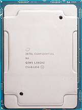
Intel Skylake Xeon gold processor
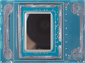
Intel Skylake Xeon gold processor, delidded

Die shot


Xeon Platinum (octal processor)[]
- Xeon Platinum non-F SKUs have three UPIs at 10.4 GT/s. Xeon Platinum F-SKUs have two UPIs at 10.4 GT/s.
- Xeon Platinum supports DDR4-2666 MHz RAM.
| Model number |
sSpec number |
Cores (threads) |
Frequency | Turbo Boost all-core/2.0 (/max. 3.0) |
L2 cache |
L3 cache |
TDP | Socket | I/O bus | Memory | Release date | Part number(s) |
Release price (USD) |
|---|---|---|---|---|---|---|---|---|---|---|---|---|---|
| Xeon Platinum 8153 |
|
16 (32) | 2 GHz | 2.3/2.8 GHz | 16 × 1 MB | 22.00 MB | 125 W
|
LGA 3647 | 3 × 10.4 GT/s QPI | 6 × DDR4-2666 | 11 July 2017 |
|
$3115 |
| Xeon Platinum 8156 |
|
4 (8) | 3.6 GHz | 3.3/3.7 GHz | 4 × 1 MB | 16.50 MB | 105 W
|
LGA 3647 | 3 × 10.4 GT/s UPI | 6 × DDR4-2666 | 11 July 2017 |
|
$7007 |
| Xeon Platinum 8158 |
|
12 (24) | 3 GHz | 2.7/3.7 GHz | 12 × 1 MB | 24.75 MB | 150 W
|
LGA 3647 | 3 × 10.4 GT/s UPI | 6 × DDR4-2666 | 11 July 2017 |
|
$7007 |
| Xeon Platinum 8160 |
|
24 (48) | 2.1 GHz | 2.8/3.7 GHz | 24 × 1 MB | 33.00 MB | 150 W
|
LGA 3647 | 3 × 10.4 GT/s UPI | 6 × DDR4-2666 | 11 July 2017 |
|
$4702 $4708 |
| Xeon Platinum 8160F |
|
24 (48) | 2.1 GHz | 2.8/3.7 GHz | 24 × 1 MB | 33.00 MB | 160 W
|
LGA 3647 | 2 × 10.4 GT/s UPI | 6 × DDR4-2666 | 11 July 2017 |
|
$4856 |
| Xeon Platinum 8160M |
|
24 (48) | 2.1 GHz | 2.8/3.7 GHz | 24 × 1 MB | 33.00 MB | 150 W
|
LGA 3647 | 3 × 10.4 GT/s UPI | 6 × DDR4-2666 | 11 July 2017 |
|
$7704 |
| Xeon Platinum 8160T |
|
24 (48) | 2.1 GHz | 2.8/3.7 GHz | 24 × 1 MB | 33.00 MB | 150 W
|
LGA 3647 | 3 × 10.4 GT/s UPI | 6 × DDR4-2666 | 11 July 2017 |
|
$4936 |
| Xeon Platinum 8163 |
|
24 (48) | 2.4 GHz | 2.7/3.1 GHz | 24 × 1 MB | 33.00 MB | 165 W
|
LGA 3647 | 3 × 10.4 GT/s UPI | 6 × DDR4-2666 | 2017 |
|
|
| Xeon Platinum 8164 |
|
26 (52) | 2 GHz | 2.7/3.7 GHz | 26 × 1 MB | 35.75 MB | 150 W
|
LGA 3647 | 3 × 10.4 GT/s UPI | 6 × DDR4-2666 | 11 July 2017 |
|
$6114 $6120 |
| Xeon Platinum 8167M |
|
26 (52) | 2 GHz | 2.4/2.4 GHz | 26 × 1 MB | 35.75 MB | 165 W
|
LGA 3647 | 3 × 10.4 GT/s UPI | 6 × DDR4-2666 | 2017 |
|
|
| Xeon Platinum 8168 |
|
24 (48) | 2.7 GHz | 3.4/3.7 GHz | 24 × 1 MB | 33.00 MB | 205 W
|
LGA 3647 | 3 × 10.4 GT/s UPI | 6 × DDR4-2666 | 11 July 2017 |
|
$5890 |
| Xeon Platinum 8170 |
|
26 (52) | 2.1 GHz | 2.8/3.7 GHz | 26 × 1 MB | 35.75 MB | 165 W
|
LGA 3647 | 3 × 10.4 GT/s UPI | 6 × DDR4-2666 | 11 July 2017 |
|
$7405 $7411 |
| Xeon Platinum 8170M |
|
26 (52) | 2.1 GHz | 2.8/3.7 GHz | 26 × 1 MB | 35.75 MB | 165 W
|
LGA 3647 | 3 × 10.4 GT/s UPI | 6 × DDR4-2666 | 11 July 2017 |
|
$10,409 |
| Xeon Platinum 8173M |
|
28 (56) | 2 GHz | 2.7/3.5 GHz | 28 × 1 MB | 38.50 MB | 165 W
|
LGA 3647 | 3 × 10.4 GT/s UPI | 6 × DDR4-2666 | 2017 |
|
|
| Xeon Platinum 8176 |
|
28 (56) | 2.1 GHz | 2.8/3.8 GHz | 28 × 1 MB | 38.50 MB | 165 W
|
LGA 3647 | 3 × 10.4 GT/s UPI | 6 × DDR4-2666 | 11 July 2017 |
|
$8790 |
| Xeon Platinum 8176F |
|
28 (56) | 2.1 GHz | 2.8/3.8 GHz | 28 × 1 MB | 38.50 MB | 173 W
|
LGA 3647 | 2 × 10.4 GT/s UPI | 6 × DDR4-2666 | Q3, 2017 |
|
$8874 |
| Xeon Platinum 8176M |
|
28 (56) | 2.1 GHz | 2.8/3.8 GHz | 28 × 1 MB | 38.50 MB | 165 W
|
LGA 3647 | 3 × 10.4 GT/s UPI | 6 × DDR4-2666 | 11 July 2017 |
|
$11,722 |
| Xeon Platinum 8180 |
|
28 (56) | 2.5 GHz | 3.2/3.8 GHz | 28 × 1 MB | 38.50 MB | 205 W
|
LGA 3647 | 3 × 10.4 GT/s UPI | 6 × DDR4-2666 | 11 July 2017 |
|
$10,009 |
| Xeon Platinum 8180M |
|
28 (56) | 2.5 GHz | 3.2/3.8 GHz | 28 × 1 MB | 38.50 MB | 205 W
|
LGA 3647 | 3 × 10.4 GT/s UPI | 6 × DDR4-2666 | 11 July 2017 |
|
$13,011 |
See also[]
References[]
- ^ "Intel Core i7-6700K Processor (8M Cache, up to 4.20 GHz)". Ark.intel.com. Retrieved January 24, 2018.
- ^ Tom's Hardware: Skylake Xeon Platforms Spotted, Purley Makes A Quiet Splash At Computex. June 3, 2016
- ^ a b c "AVX-512 SIMD enabled only on Xeon models of SkyLake". Bits and Chips.
- ^ a b "Skylake processors for the PC will not support the AVX-512". Hardware-boom.com. March 3, 2015. Retrieved January 24, 2018.
- ^ Cutress, Ian. "The Intel Skylake Mobile and Desktop Launch, with Architecture Analysis". Anandtech.com. Retrieved September 18, 2015.
- ^ a b "The Compute Architecture of Intel® Processor Graphics Gen9" (PDF). Software.intel.com. Retrieved January 24, 2018.
- ^ "Intel® 64 and IA-32 Architectures Optimization Reference Manual" (PDF). Intel.com. Retrieved January 24, 2018.
- ^ "Intel Unleashes Next-Gen Enthusiast Desktop PC Platform at Gamescom". Intel Newsroom. Retrieved August 5, 2015.
- ^ Demerjian, Charlie (March 31, 2011). "After Intel's Haswell comes Broadwell". Semiaccurate.com. Retrieved January 4, 2012.
- ^ "Intel Presentation: 22nm Details" (PDF). Retrieved January 4, 2012.
- ^ Darren Allan (August 31, 2016). "Intel's latest CPUs will only support Windows 10". Tech Radar. Retrieved June 8, 2017.
- ^ "There's a patch to reinstate Windows 7 & 8.1 on Kaby Lake CPUs | TheINQUIRER". April 20, 2017. Archived from the original on April 20, 2017. Retrieved March 9, 2020.
{{cite web}}: CS1 maint: unfit URL (link) - ^ pilao (March 3, 2020), zeffy/wufuc, retrieved March 9, 2020
- ^ Przemysław (February 9, 2020), p-lider/WuaCpuFix, retrieved March 9, 2020
- ^ "6th Generation Intel® Core i7-6700K and i5-6600K Processors". Intel. Retrieved May 25, 2018.
- ^ "6th Generation Intel® Processor Family". Intel. Retrieved May 25, 2018.
- ^ "Why Intel calls Skylake a 6th-generation CPU". PCWorld. Retrieved May 25, 2018.
- ^ http://qdms.intel.com/dm/i.aspx/EED3D500-FB5C-47A2-82E1-BF8DF2E0EF11/PCN116799-00.pdf[bare URL PDF]
- ^ "Intel in Israel: A Old Relationship Faces New Criticism". Knowledge.wharton.upenn.edu. Retrieved January 24, 2018.
- ^ "The many tricks Intel Skylake uses to go faster and use less power". Ars Technica. Condé Nast. August 19, 2015. Retrieved November 7, 2021.
- ^ Intel Introduced its 6th Generation Intel Core Published September 2, 2015, techtime.co.il
- ^ "Intel announces Skylake microarchitecture". Cpu-world.com. Retrieved January 24, 2018.
- ^ "Intel to Debut its Core Skylake Processors at Gamescom 2015". TechPowerUp.
- ^ "Intel Corporation Launching Broadwell, Skylake Chips Back to Back". ValueWalk. Retrieved October 17, 2014.
- ^ Ryan Smith. "AnandTech – Intel's 14nm Technology in Detail". Anandtech.com. Retrieved January 24, 2018.
- ^ "Intel Broadwell and Skylake client CPUs both launching in 2015". Hexus.net. Retrieved January 24, 2018.
- ^ a b "Intel's 14nm puzzle: As Skylake details leak, everybody asks – is the chip coming in 2015 or not?". ExtremeTech. July 14, 2014. Retrieved October 17, 2014.
- ^ Piyush Arora (October 15, 2014). "Intel: Skylake Development Appears To Be On Schedule". Seekingalpha.com. Retrieved January 24, 2018.
- ^ "Intel puts a stop to overclocking on non-K Skylake CPUs". PC Gamer. Retrieved February 9, 2016.
- ^ "Intel Skylake Non-K OC KOed by ASRock". Hexus.net. Retrieved February 9, 2016.
- ^ "Non-K overclocking". hwbot.org. Retrieved May 5, 2021.
- ^ "BCLK Overclocking Intel's non-K Skylake Processors: Coming Soon". Anandtech.com. Retrieved February 9, 2016.
- ^ "It's official: Intel shuts down the cheap overclocking party by closing Skylake loophole". PCWorld. February 8, 2016. Retrieved February 9, 2016.
- ^ "Yes, you can overclock cheap Intel Skylake chips". PC World. December 11, 2015. Retrieved February 9, 2016.
- ^ "New ASRock motherboards sport external clock generators for Intel CPU overclocking |". ExtremeTech. Retrieved April 10, 2016.
- ^ 株式会社インプレス (April 7, 2016). "独自OC機能を備えたH170マザーがASRockから登場、計2モデル - AKIBA PC Hotline!". AKIBA PC Hotline! (in Japanese). Retrieved April 10, 2016.
- ^ "Skylake users given 18 months to upgrade to Windows 10". Ars Technica. January 16, 2016. Retrieved January 16, 2016.
- ^ Bott, Ed. "Microsoft updates support policy: New CPUs will require Windows 10". ZDNet.com. CBS Interactive. Retrieved January 16, 2016.
- ^ "Skylake support on Windows 7 and 8.1 given a one-year extension". Ars Technica. March 18, 2016. Retrieved March 18, 2016.
- ^ "Microsoft backtracks on Windows 7 support deadline". Computerworld.com. March 18, 2016. Retrieved March 18, 2016.
- ^ Larsen, Shad (August 11, 2016). "Updates to Silicon Support Policy for Windows". Windows business blog. Microsoft. Archived from the original on April 25, 2017. Retrieved May 9, 2017.
- ^ Jo Foley, Mary (August 11, 2016). "Microsoft extends again support for Windows 7, 8.1 Skylake-based devices". ZDNet. CBS Interactive. Retrieved May 9, 2017.
- ^ "There's a patch to reinstate Windows 7 & 8.1 on Kaby Lake CPUs". Theinquirer.net. Archived from the original on December 22, 2019. Retrieved January 24, 2018.
{{cite web}}: CS1 maint: unfit URL (link) - ^ "Linux 4.11 To Enable Frame-Buffer Compression By Default For Skylake+ - Phoronix". Phoronix.com.
- ^ "OpenBSD 6.2". Retrieved October 10, 2018.
- ^ "Windows processor requirements Windows 11 supported Intel processors". docs.microsoft.com. Retrieved October 5, 2021.
{{cite web}}: CS1 maint: url-status (link) - ^ "Update on Windows 11 minimum system requirements". Windows Insider Blog. June 28, 2021. Retrieved October 5, 2021.
{{cite web}}: CS1 maint: url-status (link) - ^ Warren, Tom (August 27, 2021). "Microsoft won't stop you installing Windows 11 on older PCs". The Verge. Retrieved October 5, 2021.
- ^ Hollister, Sean (September 21, 2021). "Windows 11 won't stop older PCs, but it might make you sign this waiver". The Verge. Retrieved October 5, 2021.
- ^ Hollister, Sean (August 28, 2021). "Microsoft is threatening to withhold Windows 11 updates if your CPU is old". The Verge. Retrieved October 5, 2021.
- ^ "Intel Skylake-S desktop CPUs expected at IDF 2015 in August". February 17, 2015.
- ^ a b c Pirzada, Syed Muhammad Usman (June 27, 2014). "Massive Intel 14nm Skylake Leak – Multiple eDRAM Configurations and Desktop Variant to have Configurable TDP". WCCFTech. WCCFTech Prvt. Ltd. Retrieved June 28, 2014.
- ^ "Intel Core Skylake CPUs Accompanied by 100-series Chipset". Techpowerup.com. Retrieved May 8, 2014.
- ^ Pirzada, Syed Muhammad Usman (June 5, 2014). "Intel to Abandon the Internal Voltage Regulator (IVR) with Skylake Microarchitecture". WCCFTech. WCCFTech Prvt. Ltd. Retrieved June 28, 2014.
- ^ "How Intel Plans to Transition Between DDR3 and DDR4 for the Mainstream". techpowerup.com. September 14, 2014. Retrieved November 19, 2014.
- ^ "Intel's 6th Generation Skylake Processors Scheduled For 2H 2015 – 5th Generation Broadwell in Spring '15, Updates 2015–2016 Mobility Roadmap". WCCFtech. November 24, 2014.
- ^ "ARK | Intel® Core i7-6700K Processor (8M Cache, up to 4.20 GHz)". Ark.intel.com. Retrieved August 6, 2015.
- ^ "[Phoronix] Intel Publishes Initial Skylake Linux Graphics Support". Phoronix.com. Retrieved January 24, 2018.
- ^ Cutress, Ian. "Intel Skylake Z170 Motherboards: A Quick Look at 55+ New Products". Anandtech.com. Retrieved August 6, 2015.
- ^ "Wire-free PCs, tablets and phones coming in 2015 says Intel". ZDNet. September 10, 2014.
- ^ "Counterclockwise: the wireless charging format wars". GSMArena. November 11, 2018.
- ^ "DRIVER VERSION: 30.0.101.1404" (PDF). Downloadmirror.intel.com. Retrieved March 8, 2022.
- ^ "Mesa 13.0 Released With Intel OpenGL 4.5, RADV Radeon Vulkan Driver". Phoronix.com.
- ^ "Intel Skylake-S CPUs and 100-series Chipsets Detailed in Apparent Leak". NDTV Gadgets. April 17, 2015.
- ^ "Skylake's graphics architecture: Intel is still gunning for dedicated GPUs -- IDF15". Retrieved August 18, 2015.
- ^ "Intel Unleashes Next-Gen Enthusiast Desktop PC Platform at Gamescom – Technology@Intel". Technology@Intel. August 5, 2015. Retrieved August 10, 2015.
- ^ "[Updated] Critical Flaw In Intel Skylake And Kaby Lake HyperThreading Discovered Requiring BIOS Microcode Fix - HotHardware". Hothardware.com. June 25, 2017. Retrieved January 24, 2018.
- ^ "Re: [RFC 09/10] x86/enter: Create macros to restrict/unrestrict Indirect Branch Speculation [LWN.net]". Lwn.net. Retrieved January 24, 2018.
- ^ Alois Kraus (June 16, 2018). "Why Skylake CPUs Are Sometimes 50% Slower – How Intel Has Broken Existing Code".
- ^ "Intel® 64 and IA-32 Architectures Optimization Reference Manual 248966-033" (PDF). June 2016.
- ^ [1][dead link]
- ^ "Intel talks up new processor releases and celebrates an anniversary". Maximumpc.com. Retrieved April 16, 2016.
- ^ a b "Intel Skylake Processors To Launch in 2H 2015 – Compatible With LGA 1151 Socket and Z170 Chipset, Will Feature DDR3 / DDR4 Memory Support". Wccftech.com. June 4, 2014. Retrieved June 9, 2014.
- ^ Howse, Brett. "Examining Intel's New Speed Shift Tech on Skylake: More Responsive Processors". Anandtech.com. Retrieved April 16, 2016.
- ^ "Skylake (client) - Microarchitectures - Intel - WikiChip". en.wikichip.org. Retrieved February 8, 2021.
- ^ "Cheat sheet for Intel Processor Trace with Linux perf and GDB at Andi Kleen's blog".
- ^ "Intel Skylake: Core i7-6700K und i5-6600K im Test". PC GAMES HARDWARE ONLINE. August 5, 2015. Retrieved August 5, 2015.
- ^ "Game Dev - Graphics API Developer's Guide For 6th Generation Intel® Core Processors | Intel® Developer Zone". Software.intel.com. Retrieved April 16, 2016.
- ^ Cutress, Ian. "The Intel 6th Gen Skylake Review: Core i7-6700K and i5-6600K Tested". Anandtech.com. Retrieved January 24, 2018.
- ^ "Intel's Cannonlake 10nm Microarchitecture is Due For 2016 – Compatible On Union Bay With Union Point PCH". Wccftech.com. June 6, 2014. Retrieved June 15, 2014.
- ^ Shilov, Anton (April 4, 2012). "Intel to Start DDR4 Usage with Server Platforms in 2014". X-bit laboratories. Archived from the original on October 12, 2013. Retrieved October 5, 2013.
- ^ "Intel Skylake Could Feature Dual DDR3/DDR4 Memory Support with Double IMCs". Techpowerup.com. September 14, 2014. Retrieved November 20, 2014.
- ^ "GIGABYTE – Motherboard – Socket 1151 – GA-Z170-HD3 DDR3 (rev. 1.0)". Retrieved September 7, 2015.
- ^ "Skylake's IMC Supports Only DDR3L". Retrieved September 29, 2015.
- ^ Kirsch, Nathan (May 5, 2014). "Intel 2015 Platform Roadmap Shows Skylake CPUs, 100 Series Chipset and DDR4". Legit Reviews. Retrieved May 8, 2014.
- ^ "Intel 14nm Skylake Desktop 'Sky Bay Platform Detailed – TDPs For DT, H-Series, U-Series, Y-Series Unveiled, Quad Core With GT4e GPU Has 95W TDP". Wccftech.com. June 5, 2014. Retrieved June 9, 2014.
- ^ "6th Generation Intel® Core Processor Family Datasheet, Vol. 1". Intel. Retrieved August 22, 2015.
- ^ "GIGABYTE – Motherboard – Socket 1151 – GA-Z170-HD3 DDR3 (rev. 1.0)". Gigabyte.com. Retrieved November 2, 2015.
- ^ "Z170-P D3 – Overview". Asus.com. Retrieved November 2, 2015.
- ^ "ASRock > Z170 Pro4/D3". Asrock.com. Retrieved November 2, 2015.
- ^ Ian Cutress (August 5, 2015s). "The Intel 6th Gen Skylake Review: Core i7-6700K and i5-6600K Tested". Anandtech.com. Retrieved January 24, 2018.
- ^ Kampman, Jeff (May 30, 2017). "Intel's Core X-series CPUs and X299 platform revealed". Tech Report. Retrieved June 1, 2017.
- ^ "Intel Core X Series Processor Overview" (PDF). Newsroom.intel.com. Retrieved January 24, 2018.
- ^ Cutress, Ian. "Intel Finalizes Skylake-X Processor Specifications: 18-Cores, 4.4 GHz Turbo, 165W on September 25th". Anandtech.com. Retrieved September 20, 2017.
- ^ "Intel Unveils Full Intel® Core X-series Processor Family Specs". Intel Newsroom. Retrieved August 7, 2017.
- ^ Cutress, Ian. "Intel's Basin Falls Skylake-X Refresh: Core i9-9980XE with up to 15% Better Power Efficiency". Anandtech.com. Retrieved October 27, 2018.
- ^ Cutress, Dr Ian. "The Intel Core i9-9990XE Review: All 14 Cores at 5.0 GHz". www.anandtech.com. Retrieved January 4, 2020.
- ^ "Intel debuts 9th-generation Core chips, including Core i9 and X-series parts, with a few twists". October 8, 2018.
- ^ "Intel® Core i7-9800X X-series Processor (16.5M Cache, up to 4.50 GHz) Product Specifications". Intel® ARK (Product Specs). Retrieved December 19, 2018.
- ^ a b c d "The Intel Xeon W Review: W-2195, W-2155, W-2123, W-2104 and W-2102 Tested". www.anandtech.com. Retrieved May 4, 2019.
- ^ a b c d "Apple's iMac Pro Xeon W are ready". WikiChip Fuse. December 24, 2017. Retrieved May 4, 2019.
External links[]
- Ung, Gordon (August 18, 2015). "Intel Skylake CPU details revealed: These faster, more power-efficient chips can even drive three 4K monitors". PC world.
- Shields, Anne (September 19, 2015). "Intel's Skylake a New Lifeline for the PC Market?". Yahoo Finance.
- Intel x86 microprocessors
- Intel microarchitectures
- Transactional memory
- X86 microarchitectures