i486
This article may require copy editing for grammar, style, cohesion, tone, or spelling. (August 2021) |
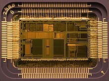 The exposed die of an Intel 486DX2 | |
| General information | |
|---|---|
| Launched | April 1989 |
| Discontinued | September 28, 2007 |
| Common manufacturer(s) |
|
| Performance | |
| Max. CPU clock rate | 16 MHz to 100 MHz |
| FSB speeds | 16 MHz to 50 MHz |
| Data width | 32 bits[1] |
| Address width | 32 bits[1] |
| Virtual address width | 32 bits (linear); 46 bits (logical)[1] |
| Architecture and classification | |
| Min. feature size | 1 µm to 0.6 µm |
| Instruction set | x86 including x87 (except for "SX" models) |
| Physical specifications | |
| Co-processor | Intel 80487SX |
| Package(s) | |
| History | |
| Predecessor | Intel 386 |
| Successor | Pentium (P5) |
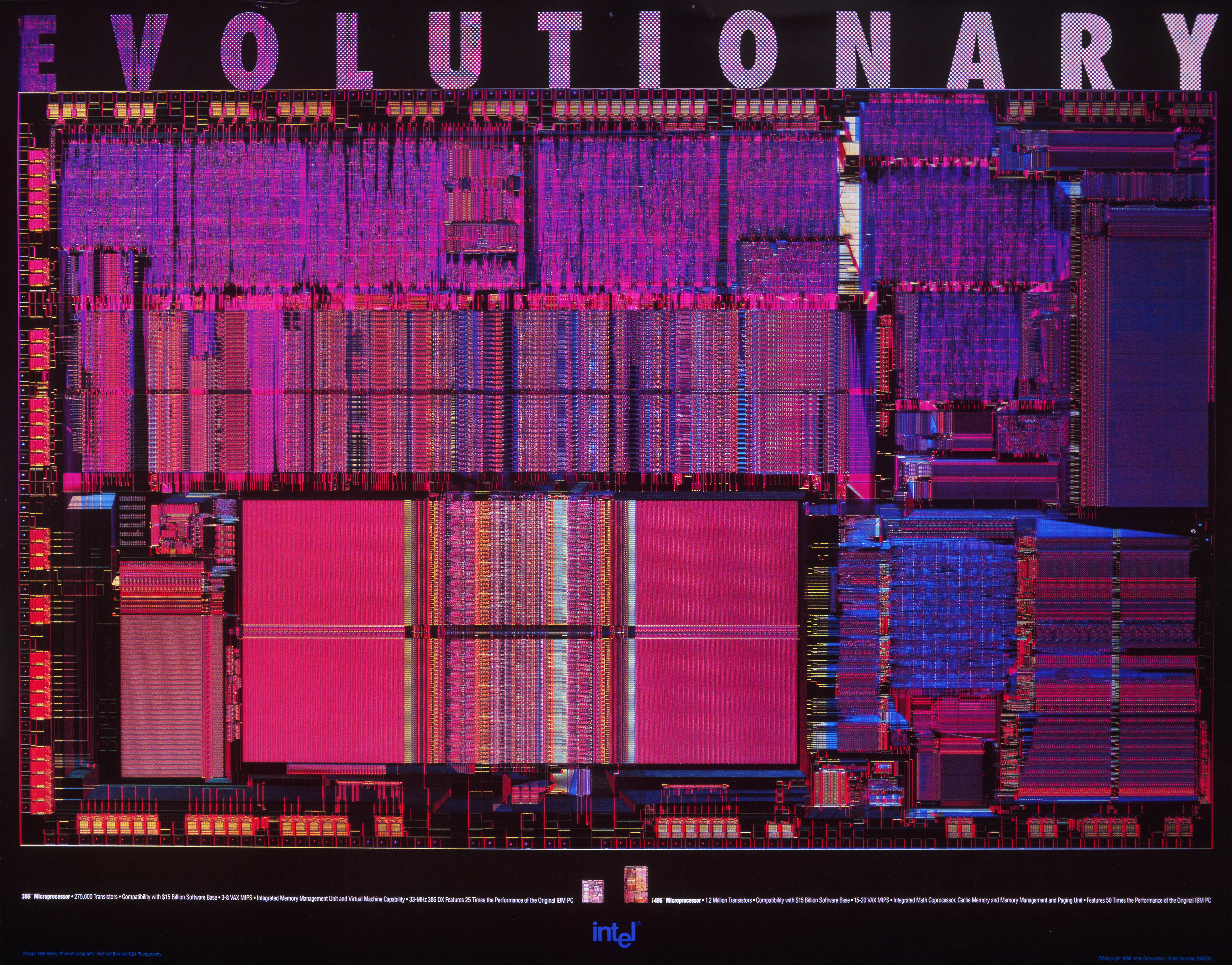
The Intel 486, officially named i486 and also known as 80486, is a higher-performance follow-up to the Intel 386 microprocessor. The i486 was introduced in 1989 and was the first tightly pipelined x86 design as well as the first x86 chip to use more than a million transistors, due to a large on-chip cache and an integrated floating-point unit. It represents a fourth generation of binary compatible CPUs since the original 8086 of 1978.
A 50 MHz i486 executes around 40 million instructions per second on average and is able to reach 50 MIPS peak performance, approximately twice as fast as the i386 or 80286 per clock cycle, thanks to its five-stage pipeline with all stages bound to a single cycle. The enhanced FPU unit on the chip was also significantly faster than the 80387 per cycle.
The i486 was succeeded by the original Pentium.
History[]
The i486 was announced at Spring Comdex in April 1989. At the announcement, Intel stated that samples would be available in the third quarter of 1989 and production quantities would ship in the fourth quarter of 1989.[2] The first i486-based PCs were announced in late 1989, but some advised that people wait until 1990 to purchase an i486 PC because there were early reports of bugs and software incompatibilities.[3]
The first major update to the i486 design came in March 1992 with the release of the 486DX2 series with an integrated math coprocessor and L1 cache.[4] It was the first time that the CPU core clock frequency was separated from the system bus clock frequency by using a dual clock multiplier, leading to the release of the 486DX2 chips at 40- and 50-MHz. The faster 66-MHz 486DX2-66 was released later in August of the same year.[4]
Despite the launch of the new fifth-generation Pentium processor in 1993, Intel continued to produce i486 processors, which led to the release of the triple-clock-rate 486DX4-100 with a 100 MHz clock speed and a L1 cache doubled to 16 KB.[4]
Earlier, Intel decided not to share its 80386 and 80486 technologies with AMD. However, AMD believed that their technology sharing extended to the 80386 as a derivative of the 80286.[4] So AMD reverse-engineered Intel 386 chip and produced the 40-MHz Am386DX-40 chip, which was cheaper and had lower power consumption than Intel's best 33-MHz version of the 386.[4] Intel attempted to prevent AMD from selling the processor, but AMD won the court battle, which allowed it to release the processor and establish itself as a competitor to Intel.[5]
AMD continued to create clones, resulting in the first-generation Am486 chip released in April 1993 with clock frequencies of 25-, 33- and 40 MHz. Subsequent second-generation Am486DX2 chips with 50-, 66- and 80-MHz clock frequencies were released the following year.[4] The Am486 series was completed with a 120-MHz DX4 chip in 1995.[4]
AMD's long-running 1987 arbitration lawsuit against Intel was settled in 1995 after an eight-year legal battle, and AMD gained access to Intel's 80486 microcode.[4] This reportedly led to the creation of two versions of AMD's 486 processor - one was reverse-engineered from Intel's microcode, and the other used AMD's microcode in a clean-room development process. However, the settlement also concluded that the 80486 would be the last Intel processor to be cloned by AMD.[4]
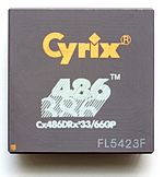
Another 486 clone manufacturer was Cyrix, which was a fabless co-processor chip maker for 80286/386 systems. The first Cyrix 486 processors, the 486SLC and 486DLC, were released in 1992 and used the 80386 package.[4] Both Texas Instruments-manufactured Cyrix processors were pin-compatible with 386SX/DX systems, which allowed them to become an upgrade option.[5] However, these chips could not match the Intel 486 processors, having only 1 KB of cache memory and no built-in math coprocessor. In 1993, Cyrix released its own Cx486DX and DX2 processors, which were closer in performance to Intel's counterparts. This led to Intel and Cyrix suing each other, with Intel going for patent infringement and Cyrix going with antitrust claims. The litigation ended in 1994 with Cyrix winning and dropping the antitrust claim.[4]
In 1995, both Cyrix and AMD began looking at a ready market for users wanting to upgrade their processors. Cyrix released a derivative 486 processor called the 5x86, based on the Cyrix M1 core, which was clocked up to 120-MHz and was an option for 486 Socket 3 motherboards.[4][5] AMD also released a 133-MHz Am5x86 upgrade chip, which was essentially an improved 80486 with double the cache and a quad multiplier that also worked with the original 486DX motherboards.[4] Am5x86 was the first processor to use AMD's performance rating and was marketed as Am5x86-P75, with claims that it was equivalent to the Pentium 75.[5] Kingston Technology company also launched a 'TurboChip' 486 system upgrade that used a 133-MHz Am5x86.[4]
This ended in Intel making a Pentium OverDrive upgrade chip for 486 motherboards, which was a modified Pentium core that ran up to 83-MHz on boards with 25- or 33-MHz front-side bus clock. OverDrive wasn't popular due to speed and price. After the Pentium series of processors gained a foothold in the market, Intel continued to produce 486 cores for industrial embedded applications and later discontinued production of i486 processors in late 2007.[4]
Improvements[]

| ||||||||||||||||||||||||||||||||||||||||||||||||||||||||||||||||||||||||||||||||||||||||||||||||||||||||||||||||||||||||||||||||||||||||||||||||||||||||||||||||
| ||||||||||||||||||||||||||||||||||||||||||||||||||||||||||||||||||||||||||||||||||||||||||||||||||||||||||||||||||||||||||||||||||||||||||||||||||||||||||||||||
| ||||||||||||||||||||||||||||||||||||||||||||||||||||||||||||||||||||||||||||||||||||||||||||||||||||||||||||||||||||||||||||||||||||||||||||||||||||||||||||||||
The instruction set of the i486 is very similar to its predecessor, the i386, with the addition of only a few extra instructions, such as CMPXCHG which implements a compare-and-swap atomic operation and XADD, a fetch-and-add atomic operation returning the original value (unlike a standard ADD which returns flags only).
From a performance point of view, the architecture of the i486 is a vast improvement over the i386. It has an on-chip unified instruction and data cache, an on-chip floating-point unit (FPU) and an enhanced bus interface unit. Due to the tight pipelining, sequences of simple instructions (such as ALU reg,reg and ALU reg,im) could sustain a single-clock-cycle throughput (one instruction completed every clock). These improvements yielded a rough doubling in integer ALU performance over the 386 at the same clock rate. A 16-MHz i486 therefore had a performance similar to a 33-MHz i386, and the older design had to reach 50 MHz to be comparable with a 25-MHz i486 part.[a]
Differences between i386 and i486[]
- An 8 KB on-chip (level 1) SRAM cache stores the most recently used instructions and data (16 KB and/or write-back on some later models). The i386 had no such internal cache but supported a slower off-chip cache (which was not a level 2 cache because there was no internal level 1 cache on the i386).
- An enhanced external bus protocol to enable cache coherency and a new burst mode for memory accesses to fill a cacheline of 16 bytes within five bus cycles. The 386 needed eight bus cycles to transfer the same amount of data.
- Tightly coupled[b] pipelining completes a simple instruction like ALU reg,reg or ALU reg,im every clock cycle (after a latency of several cycles). The 386 needed two clock cycles to do this.
- Integrated FPU (disabled or absent in SX models) with a dedicated local bus; together with faster algorithms on more extensive hardware than in the i387, this performs floating-point calculations faster compared to the i386/i387 combination.
- Improved MMU performance.
- New instructions: XADD, BSWAP, CMPXCHG, INVD, WBINVD, INVLPG.
Just as in the i386, a simple flat 4 GB memory model could be implemented by setting all "segment selector" registers to a neutral value in protected mode, or setting (the same) "segment registers" to zero in real mode, and using only the 32-bit "offset registers" (x86-terminology for general CPU registers used as address registers) as a linear 32-bit virtual address bypassing the segmentation logic. Virtual addresses were then normally mapped onto physical addresses by the paging system except when it was disabled. (Real mode had no virtual addresses.) Just as with the i386, circumventing memory segmentation could substantially improve performance in some operating systems and applications.
On a typical PC motherboard, either four matched 30-pin (8-bit) SIMMs or one 72-pin (32-bit) SIMM per bank were required to fit the i486's 32-bit data bus. The address bus used 30-bits (A31..A2) complemented by four byte-select pins (instead of A0,A1) to allow for any 8/16/32-bit selection. This meant that the limit of directly addressable physical memory was 4 gigabytes as well (230 32-bit words = 232 8-bit words).
Models[]
There are several suffixes and variants. (see the table). Other variants include:
- Intel RapidCAD: a specially packaged Intel 486DX and a dummy floating-point unit (FPU) designed as pin-compatible replacements for an i386 processor and 80387 FPU.
- i486SL-NM: i486SL based on i486SX.
- i487SX (P23N): i486DX with one extra pin sold as an FPU upgrade to i486SX systems; When the i487SX was installed, it ensured that an i486SX was present on the motherboard but disabled it, taking over all of its functions.
- i486 OverDrive (P23T/P24T): i486SX, i486SX2, i486DX2 or i486DX4. Marked as upgrade processors, some models had different pinouts or voltage-handling abilities from "standard" chips of the same speed stepping. Fitted to a coprocessor or "OverDrive" socket on the motherboard, worked the same as the i487SX.
The specified maximal internal clock frequency (on Intel's versions) ranged from 16 to 100 MHz. The 16 MHz i486SX model was used by Dell Computers.
One of the few i486 models specified for a 50 MHz bus (486DX-50) initially had overheating problems and was moved to the 0.8-micrometre fabrication process. However, problems continued when the 486DX-50 was installed in local-bus systems due to the high bus speed, making it rather unpopular with mainstream consumers, as local-bus video was considered a requirement at the time, though it remained popular with users of EISA systems. The 486DX-50 was soon eclipsed by the clock-doubled i486DX2, which although running the internal CPU logic at twice the external bus speed (50 MHz), was nevertheless slower due to the external bus running at only 25 MHz. The i486DX2 at 66 MHz (with 33 MHz external bus) was faster than the 486DX-50, overall.
More powerful i486 iterations such as the OverDrive and DX4 were less popular (the latter available as an OEM part only), as they came out after Intel had released the next-generation Pentium processor family. Certain steppings of the DX4 also officially supported 50 MHz bus operation, but it was a seldom-used feature.
Model CPU/bus
clock speedVoltage L1 cache* Introduced Notes 


i486DX (P4) 20, 25 MHz
33 MHz
50 MHz5 V 8 KB WT April 1989
May 1990
June 1991The original chip without clock multiplier 
i486SL 20, 25, 33 MHz 5 V or 3.3 V 8 KB WT November 1992 Low-power version of the i486DX, reduced VCore, SMM (System Management Mode), stop clock, and power-saving features — mainly for use in portable computers 
i486SX (P23) 16, 20, 25 MHz
33 MHz5 V 8 KB WT September 1991
September 1992An i486DX with the FPU part disabled or missing. Early variants were parts with disabled (defective) FPUs.[6] Later versions had the FPU removed from the die to reduce area and hence cost. 
i486DX2 (P24) 40/20, 50/25 MHz
66/33 MHz5 V 8 KB WT March 1992
August 1992The internal processor clock runs at twice the clock rate of the external bus clock i486DX-S (P4S) 33 MHz; 50 MHz 5 V or 3.3 V 8 KB WT June 1993 SL Enhanced 486DX 
i486DX2-S (P24S) 40/20 MHz,
50/25 MHz,
(66/33 MHz)5 V or 3.3 V 8 KB WT June 1993 
i486SX-S (P23S) 25, 33 MHz 5 V or 3.3 V 8 KB WT June 1993 SL Enhanced 486SX 
i486SX2 50/25, 66/33 MHz 5 V 8 KB WT March 1994 i486DX2 with the FPU disabled 

IntelDX4 (P24C) 75/25, 100/33 MHz 3.3 V 16 KB WT March 1994 Designed to run at triple clock rate (not quadruple, as often believed; the DX3, which was meant to run at 2.5× the clock speed, was never released). DX4 models that featured write-back cache were identified by an "&EW" laser-etched into their top surface, while the write-through models were identified by "&E". 
i486DX2WB (P24D) 50/25 MHz,
66/33 MHz5 V 8 KB WB October 1994 Enabled write-back cache. 
IntelDX4WB 100/33 MHz 3.3 V 16 KB WB October 1994 i486DX2 (P24LM) 90/30 MHz,
100/33 MHz2.5–2.9 V 8 KB WT 1994 
i486GX up to 33 MHz 3.3 V 8 KB WT Embedded ultra-low-power CPU with all features of the i486SX and 16-bit external data bus. This CPU is for embedded battery-operated and hand-held applications.


*WT = write-through cache strategy, WB = write-back cache strategy
Other makers of 486-like CPUs[]
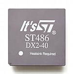

Processors compatible with the i486 have been produced by other companies such as IBM, Texas Instruments, AMD, Cyrix, UMC, and STMicroelectronics (formerly SGS-Thomson). Some were clones (identical at the microarchitectural level), others were clean room implementations of the Intel instruction set. (IBM's multiple-source requirement is one of the reasons behind its x86 manufacturing since the 80286.) The i486 was, however, covered by many of Intel's patents covering new R&D as well as that of the prior i386. Intel and IBM have broad cross-licenses of these patents, and AMD was granted rights to the relevant patents in the 1995 settlement of a lawsuit between the companies.[7]
AMD produced several clones of the i486 using a 40 MHz bus (486DX-40, 486DX/2-80, and 486DX/4-120) which had no equivalent available from Intel, as well as a part specified for 90 MHz, using a 30 MHz external clock, that was sold only to OEMs. The fastest running i486-compatible CPU, the Am5x86, ran at 133 MHz and was released by AMD in 1995. 150 MHz and 160 MHz parts were planned but never officially released.
Cyrix made a variety of i486-compatible processors, positioned at the cost-sensitive desktop and low-power (laptop) markets. Unlike AMD's 486 clones, the Cyrix processors were the result of clean-room reverse engineering. Cyrix's early offerings included the 486DLC and 486SLC, two hybrid chips which plugged into 386DX or SX sockets respectively, and offered 1 KB of cache (versus 8 KB for the then-current Intel/AMD parts). Cyrix also made "real" 486 processors, which plugged into the i486's socket and offered 2 or 8 KB of cache. Clock-for-clock, the Cyrix-made chips were generally slower than their Intel/AMD equivalents, though later products with 8 KB caches were more competitive, if late to market.
The Motorola 68040, while not compatible with the i486, was often positioned as its equivalent in features and performance. Clock-for-clock basis the Motorola 68040 could significantly outperform the Intel 486 chip.[8][9] However, the i486 had the ability to be clocked significantly faster without suffering from overheating problems. The Motorola 68040 performance lagged behind the later production i486 systems.[citation needed]
Motherboards and buses[]
This section does not cite any sources. (March 2021) |

Early i486-based computers were equipped with several ISA slots (using an emulated PC/AT-bus) and sometimes one or two 8-bit-only slots (compatible with the PC/XT-bus).[c] Many motherboards enabled overclocking of these up from the default 6 or 8 MHz to perhaps 16.7 or 20 MHz (half the i486 bus clock) in several steps, often from within the BIOS setup. Especially older peripheral cards normally worked well at such speeds as they often used standard MSI chips instead of slower (at the time) custom VLSI designs. This could give significant performance gains (such as for old video cards moved from a 386 or 286 computer, for example). However, operation beyond 8 or 10 MHz could sometimes lead to stability problems, at least in systems equipped with SCSI or sound cards.
Some motherboards came equipped with a 32-bit bus called EISA that was backward compatible with the ISA-standard. EISA offered a number of attractive features such as increased bandwidth, extended addressing, IRQ sharing, and card configuration through software (rather than through jumpers, DIP switches, etc.) However, EISA cards were expensive and therefore mostly employed in servers and workstations. Consumer desktops often used the simpler but faster VESA Local Bus (VLB), unfortunately somewhat prone to electrical and timing-based instability; typical consumer desktops had ISA slots combined with a single VLB slot for a video card. VLB was gradually replaced by PCI during the final years of the i486 period. Few Pentium class motherboards had VLB support as VLB was based directly on the i486 bus; it was no trivial matter adapting it to the quite different P5 Pentium-bus. ISA persisted through the P5 Pentium generation and was not completely displaced by PCI until the Pentium III era.
Late i486 boards were normally equipped with both PCI and ISA slots, and sometimes a single VLB slot as well. In this configuration, VLB or PCI throughput suffered depending on how buses were bridged. Initially, the VLB slot in these systems was usually fully compatible only with video cards (quite fitting as "VESA" stands for Video Electronics Standards Association); VLB-IDE, multi I/O, or SCSI cards could have problems on motherboards with PCI slots. The VL-Bus operated at the same clock speed as the i486-bus (basically being a local bus) while the PCI bus also usually depended on the i486 clock but sometimes had a divider setting available via the BIOS. This could be set to 1/1 or 1/2, sometimes even 2/3 (for 50 MHz CPU clocks). Some motherboards limited the PCI clock to the specified maximum of 33 MHz and certain network cards depended on this frequency for correct bit-rates. The ISA clock was typically generated by a divider of the CPU/VLB/PCI clock (as implied above).
One of the earliest complete systems to use the i486 chip was the Apricot VX FT, produced by British hardware manufacturer Apricot Computers. Even overseas in the United States it was popularized as "The World's First 486" in the September 1989 issue of Byte magazine (shown right).
Later i486 boards also supported Plug-And-Play, a specification designed by Microsoft that began as a part of Windows 95 to make component installation easier for consumers.
Obsolescence[]
The AMD Am5x86, up to 133 MHz, and Cyrix Cx5x86, up to 120 MHz, were the last i486 processors that were often used in late-generation i486 motherboards with PCI slots and 72-pin SIMMs that are designed to be able to run Windows 95, and also often used as upgrades for older 80486 motherboards. While the Cyrix Cx5x86 faded quite quickly when the Cyrix 6x86 took over, the AMD Am5x86 was important during the time when the AMD K5 was delayed.
Computers based on the i486 remained popular through the late 1990s, serving as low-end processors for entry-level PCs. Production for traditional desktop and laptop systems ceased in 1998, when Intel introduced the Celeron brand as a modern replacement for the aging chip, though it continued to be produced for embedded systems through the late 2000s.
In the general-purpose desktop computer role, i486-based machines remained in use into the early 2000s, especially as Windows 95 to Windows 98, and Windows NT 4.0 were the latest Microsoft operating systems to officially support installation on an i486-based system.[10][11] However, as Windows 95-98 and Windows NT 4.0 were eventually overtaken by newer operating systems, i486 systems likewise fell out of use. Still, some i486 machines remained in use, mostly for backward compatibility with older programs (most notably games), especially since many of them have problems running on newer operating systems. However, DOSBox is also available for current operating systems and provides emulation of the i486 instruction set, as well as full compatibility with most DOS-based programs.[12]
Although the i486 was eventually overtaken by the Pentium for personal computer applications, Intel had continued production for use in embedded systems. In May 2006 Intel announced that production of the i486 would stop at the end of September 2007.[13]
See also[]
- List of Intel microprocessors
- Motorola 68040, although not compatible, was often positioned as the Motorola equivalent to the Intel 486 in terms of performance and features.
- VL86C020, ARM3 core of similar time frame and comparable MIPS performance on integer code (25 MHz for both), with 310,000 transistors (in a 1.5 µm process) instead of 1 million
Notes[]
- ^ The "low-end" 16 and 25 MHz i486 parts did not use a clock multiplier and are therefore comparable to a 386/286 clock by clock.
- ^ The 386, 286, and even the 8086 all had overlapping fetch, decode, execution (calculation), and write back; however, tightly pipelined usually means that all stages perform their respective duties within the same length time slot. In contrast loosely pipelined implies that some kind of buffering is used to decouple the units and allow them to work more independently. Both the original 8086 and the x86-chips of today are "loosely pipelined" in this sense, while the i486 and the original Pentium worked in a "tightly pipelined" manner for typical instructions. This included most "CISC" type instructions as well as the simple load/store-free "RISC-like" ones, although the most complex also used some dedicated microcode control.
- ^ In general, 8-bit ISA slots in these systems were implemented just by leaving off the shorter "C"/"D" connector of the slot, though the copper traces for a 16-bit slot were still there on the motherboard; the computer could tell no difference between an 8-bit ISA adapter in such a slot and the same adapter in a 16-bit slot, and there were still enough 8-bit adapters in circulation that vendors figured they could save money on a few connectors this way. Also, leaving off the 16-bit extension to the ISA connector allowed use of some early 8-bit ISA cards that otherwise could not be used due to the PCB "skirt" hanging down into that 16-bit extension space. IBM was the first to do this in the IBM AT.
References[]
- ^ Jump up to: a b c Intel (July 1997). Embedded Intel486 Processor Hardware Reference Manual (273025-001).
- ^ 486 32-bit CPU breaks new ground in chip density and operating performance. (Intel Corp.) (product announcement) EDN | May 11, 1989 | Pryce, Dave
- ^ Lewis, Peter H. (October 22, 1989). "THE EXECUTIVE COMPUTER; The Race to Market a 486 Machine". The New York Times. Retrieved May 5, 2010.
- ^ Jump up to: a b c d e f g h i j k l m n o Yates, Darren (November 2020). "Four. Eight. Six". APC. No. 486. Future Publishing. pp. 52–55. ISSN 0725-4415.
- ^ Jump up to: a b c d Lilly, Paul (April 14, 2009). "A Brief History of CPUs: 31 Awesome Years of x86". PC Gamer. Retrieved August 7, 2021.
- ^ Newnes 8086 Family Pocket Book – Ian Sinclair (ISBN 0 4349 1872 5)
- ^ "AMD-Intel Litigation History". yannalaw.com.
- ^ "CISC: The Intel 80486 vs. The Motorola MC68040". July 1992. Retrieved May 20, 2013.
- ^ 68040 Microprocessor Archived February 16, 2012, at the Wayback Machine
- ^ "Minimum Hardware Requirements for a Windows 98 Installation". January 24, 2001. Archived from the original on December 5, 2004.
- ^ "Windows NT 4.0 Workstation" (in German). WinHistory.de.
- ^ "System Requirements". DOSBox.com.
- ^ Tony Smith (May 18, 2006). "Intel cashes in ancient chips. i386, i486, i960 finally for the chop". HARDWARE. Archived from the original on August 22, 2011. Retrieved May 20, 2012.
External links[]
- Intel486 datasheets
- Intel i486 DX images and descriptions at cpu-collection.de
- Die photo of Intel 386DX
| show Authority control |
|---|
- Intel microprocessors
- Computer-related introductions in 1989
- Intel x86 microprocessors