Tunnel diode
 1N3716 tunnel diode (with 0.1" jumper for scale) | |
| Type | Passive |
|---|---|
| Working principle | Quantum mechanical effect called tunneling |
| Invented | Leo Esaki Yuriko Kurose[1] Takashi Suzuki[2][3] |
| First production | Sony |
| Pin configuration | anode and cathode |
| Electronic symbol | |
 | |

A tunnel diode or Esaki diode is a type of semiconductor diode that has effectively "negative resistance" due to the quantum mechanical effect called tunneling. It was invented in August 1957 by Leo Esaki, Yuriko Kurose, and Takashi Suzuki when they were working at Tokyo Tsushin Kogyo, now known as Sony.[1][2][3][4] In 1973, Esaki received the Nobel Prize in Physics, jointly with Brian Josephson, for discovering the electron tunneling effect used in these diodes. Robert Noyce independently devised the idea of a tunnel diode while working for William Shockley, but was discouraged from pursuing it.[5] Tunnel diodes were first manufactured by Sony in 1957,[6] followed by General Electric and other companies from about 1960, and are still made in low volume today.[7]
Tunnel diodes have a heavily doped positive-to-negative (P-N) junction that is about 10 nm (100 Å) wide. The heavy doping results in a broken band gap, where conduction band electron states on the N-side are more or less aligned with valence band hole states on the P-side. They are usually made from germanium, but can also be made from gallium arsenide and silicon materials.
Uses[]
Their "negative" differential resistance in part of their operating range allows them to function as oscillators and amplifiers, and in switching circuits using hysteresis. They are also used as frequency converters and detectors.[8]:7–35 Their low capacitance allows them to function at microwave frequencies, far above the range of ordinary diodes and transistors.

Due to their low output power, tunnel diodes are not widely used: Their RF output is limited to a few hundred milliwatts due to their small voltage swing. In recent years, however, new devices that use the tunneling mechanism have been developed. The resonant-tunneling diode (RTD) has achieved some of the highest frequencies of any solid-state oscillator.[9]
Another type of tunnel diode is a metal–insulator–insulator–metal (MIIM) diode, where an additional insulator layer allows "step tunneling" for more precise control of the diode.[10] There is also a metal–insulator–metal (MIM) diode, but due to inherent sensitivities, its present application appears to be limited to research environments.[11]
Forward bias operation[]
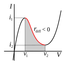
Under normal forward bias operation, as voltage begins to increase, electrons at first tunnel through the very narrow P-N junction barrier and fill electron states in the conduction band on the N-side which become aligned with empty valence band hole states on the P-side of the P-N junction. As voltage increases further, these states become increasingly misaligned, and the current drops. This is called negative differential resistance because current decreases with increasing voltage. As voltage increases beyond a fixed transition point, the diode begins to operate as a normal diode, where electrons travel by conduction across the P-N junction, and no longer by tunneling through the P–N junction barrier. The most important operating region for a tunnel diode is the "negative resistance" region. Its graph is different from normal P-N junction diode.
Reverse bias operation[]
When used in the reverse direction, tunnel diodes are called back diodes (or backward diodes) and can act as fast rectifiers with zero offset voltage and extreme linearity for power signals (they have an accurate square law characteristic in the reverse direction). Under reverse bias, filled states on the P-side become increasingly aligned with empty states on the N-side, and electrons now tunnel through the P-N junction barrier in reverse direction.
Technical comparisons[]

In a conventional semiconductor diode, conduction takes place while the P-N junction is forward biased and blocks current flow when the junction is reverse biased. This occurs up to a point known as the "reverse breakdown voltage" at which point conduction begins (often accompanied by destruction of the device). In the tunnel diode, the dopant concentrations in the P and N layers are increased to a level such that the reverse breakdown voltage becomes zero and the diode conducts in the reverse direction. However, when forward-biased, an effect occurs called quantum mechanical tunneling which gives rise to a region in its voltage vs. current behavior where an increase in forward voltage is accompanied by a decrease in forward current. This "negative resistance" region can be exploited in a solid state version of the dynatron oscillator which normally uses a tetrode thermionic valve (vacuum tube).
Applications[]
The tunnel diode showed great promise as an oscillator and high-frequency threshold (trigger) device since it operated at frequencies far greater than the tetrode could: well into the microwave bands. Applications of tunnel diodes included local oscillators for UHF television tuners, trigger circuits in oscilloscopes, high-speed counter circuits, and very fast-rise time pulse generator circuits. In 1977, the Intelsat V satellite receiver used a microstrip tunnel diode amplifier (TDA) front-end in the 14–15.5 GHz frequency band. Such amplifiers were considered state-of-the-art, with better performance at high frequencies than any transistor-based front end.[12] The tunnel diode can also be used as a low-noise microwave amplifier.[8]:13–64 Since its discovery, more conventional semiconductor devices have surpassed its performance using conventional oscillator techniques. For many purposes, a three-terminal device, such as a field-effect transistor, is more flexible than a device with only two terminals. Practical tunnel diodes operate at a few milliamperes and a few tenths of a volt, making them low-power devices.[13] The Gunn diode has similar high frequency capability and can handle more power.
Tunnel diodes are also more resistant to ionizing radiation than other diodes.[citation needed] This makes them well suited to higher radiation environments such as those found in space.
Longevity[]
Tunnel diodes are susceptible to damage by overheating, and thus special care is needed when soldering them.
Tunnel diodes are notable for their longevity, with devices made in the 1960s still functioning. Writing in Nature, Esaki and coauthors state that semiconductor devices in general are extremely stable, and suggest that their shelf life should be "infinite" if kept at room temperature. They go on to report that a small-scale test of 50 year-old devices revealed a "gratifying confirmation of the diode's longevity". As noticed on some samples of Esaki diodes, the gold-plated iron pins can in fact corrode and short out to the case. This can usually be diagnosed and treated with simple peroxide / vinegar technique normally used for repairing phone PCBs and the diode inside normally still works.[14]
Surplus Russian components are also reliable and often can be purchased for a few pence, despite original cost being in the £30–50 range. The units typically sold are GaAs based and have a Ipk⁄Iv ratio of 5:1 at around 1–20 mA Ipk, and so should be protected against overcurrent.[15]
See also[]
- Avalanche diode
- Gunn diode
- IMPATT diode
- Lambda diode
- Resonant-tunneling diode
- Tunnel junction
- Zener diode
References[]
- ^ Jump up to: a b "Diode type semiconductor device". United States patent. 3,033,714.
- ^ Jump up to: a b Esaki, L.; Kurose, Y.; Suzuki, T. (1957). "Ge P-N Junction のInternal Field Emission". 日本物理学会年会講演予稿集. 12 (5): 85.
- ^ Jump up to: a b "Chapter 9: The Model 2T7 Transistor". www.sony.net. Sony History. Sony Global. Retrieved 4 April 2018.
- ^ Esaki, Leo (15 January 1958). "New Phenomenon in Narrow Germanium p−n Junctions". Physical Review. 109 (2): 603–604. Bibcode:1958PhRv..109..603E. doi:10.1103/PhysRev.109.603.
- ^ Berlin, Leslie (2005). The Man Behind the Microchip: Robert Noyce and the Invention of Silicon Valley. Oxford, UK: Oxford University Press. ISBN 0-19-516343-5.
- ^ ソニー半導体の歴史 (in Japanese). Archived from the original on 2 February 2009.
- ^ Rostky, George. "Tunnel diodes: the transistor killers". EE Times. Archived from the original on 7 January 2010. Retrieved 2 October 2009.
- ^ Jump up to: a b Fink, Donald G., ed. (1975). Electronic Engineers Handbook. New York, NY: McGraw Hill. ISBN 0-07-020980-4.
- ^ Brown, E.R.; Söderström, J.R.; Parker, C.D.; Mahoney, L.J.; Molvar, K.M.; McGill, T.C. (18 March 1991). "Oscillations up to 712 GHz in InAs/AlSb resonant-tunneling diodes" (PDF). Applied Physics Letters. 58 (20): 2291. Bibcode:1991ApPhL..58.2291B. doi:10.1063/1.104902. ISSN 0003-6951.
- ^ Conley, John (4 September 2013). "Electronics advance moves closer to a world beyond silicon". OSU College of Engineering.
- ^ "The MIM diode: Another challenger for the electronics crown". SciTechStory. 19 November 2010. Archived from the original on 24 December 2016. Retrieved 4 January 2017.
- ^ Mott, R.C. (November 1978). "Intelsat V 14 GHz tunnel diode noise figure study". COMSAT Technical Review. 8: 487–507. Bibcode:1978COMTR...8..487M. ISSN 0095-9669.
- ^ Turner, L.W., ed. (1976). Electronics Engineer's Reference Book (4th ed.). London, UK: Newnes-Butterworth. pp. 8–18. ISBN 0-408-00168-2.
- ^ Esaki, Leo; Arakawa, Yasuhiko; Kitamura, Masatoshi (2010). "Esaki diode is still a radio star, half a century on". Nature. 464 (7285): 31. Bibcode:2010Natur.464Q..31E. doi:10.1038/464031b. PMID 20203587.
- ^ "Russian tunnel diodes". w140.com. TekWiki. Retrieved 4 April 2018.
External links[]
| Wikimedia Commons has media related to Tunnel diodes. |
| show Sony |
|---|
| show Authority control |
|---|
- Diodes
- Japanese inventions
- 1957 in technology
- 1957 introductions